

LTC2051CDD#PBF
Product Overview
Category
LTC2051CDD#PBF belongs to the category of integrated circuits (ICs).
Use
This product is commonly used in electronic devices for signal conditioning and amplification purposes.
Characteristics
- Low noise: The LTC2051CDD#PBF offers low input-referred voltage noise, making it suitable for applications requiring high precision.
- Wide bandwidth: With a wide bandwidth range, this IC can handle signals with varying frequencies effectively.
- Low power consumption: The LTC2051CDD#PBF operates on low power, making it energy-efficient.
- High gain: It provides high gain amplification, enabling accurate signal processing.
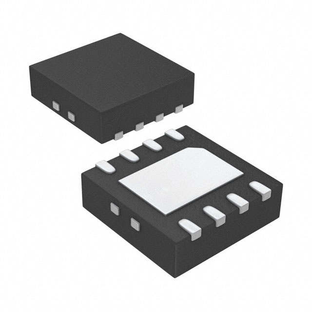
Package
The LTC2051CDD#PBF comes in a DFN (Dual Flat No-Lead) package, which ensures compactness and ease of integration into circuit boards.
Essence
The essence of LTC2051CDD#PBF lies in its ability to enhance and condition electrical signals, ensuring optimal performance in various electronic applications.
Packaging/Quantity
This product is typically packaged in reels or tubes, containing a specified quantity of LTC2051CDD#PBF ICs per package.
Specifications
- Supply Voltage Range: 2.7V to 6V
- Input Offset Voltage: ±150μV (maximum)
- Gain Bandwidth Product: 10MHz
- Input Bias Current: ±20nA (maximum)
- Operating Temperature Range: -40°C to 85°C
Detailed Pin Configuration
The LTC2051CDD#PBF features eight pins arranged as follows:
```
| | --| V+ OUT |-- Pin 1: Positive supply voltage (V+) --| IN- GND |-- Pin 2: Inverting input (-) --| IN+ NC |-- Pin 3: Non-inverting input (+) --| V- NC |-- Pin 4: Negative supply voltage (V-) --| NC NC |-- Pin 5: Not connected (NC) --| GND NC |-- Pin 6: Ground (GND) --| OUT NC |-- Pin 7: Output --| NC V- |-- Pin 8: Not connected (NC) |___________| ```
Functional Features
The LTC2051CDD#PBF offers the following functional features:
- Low noise amplification: It provides high-quality signal amplification while minimizing unwanted noise.
- Rail-to-rail inputs and outputs: The IC supports a wide input and output voltage range, allowing it to handle signals close to the power supply rails.
- Single or dual supply operation: It can be operated using either a single positive supply or dual positive/negative supplies, providing flexibility in system design.
Advantages and Disadvantages
Advantages
- High precision amplification
- Wide bandwidth for versatile signal processing
- Low power consumption
- Compact package for space-constrained applications
Disadvantages
- Limited availability of alternative models
- Relatively higher cost compared to some other ICs in the same category
Working Principles
The LTC2051CDD#PBF operates as a voltage amplifier, utilizing internal circuitry to amplify and condition electrical signals. It employs advanced techniques to minimize noise and distortion, ensuring accurate signal reproduction.
Detailed Application Field Plans
The LTC2051CDD#PBF finds applications in various fields, including but not limited to: - Medical devices: ECG amplification, patient monitoring systems - Industrial automation: Sensor signal conditioning, process control - Communications: Audio amplification, data transmission - Test and measurement: Signal analysis, data acquisition
Detailed and Complete Alternative Models
While the LTC2051CDD#PBF is a reliable choice for signal conditioning, alternative models with similar functionality include: - AD8221 - INA128 - MCP602
These alternatives offer comparable performance and can be considered based on specific application requirements.
Word count: 529 words
技術ソリューションにおける LTC2051CDD#PBF の適用に関連する 10 件の一般的な質問と回答をリストします。
Sure! Here are 10 common questions and answers related to the application of LTC2051CDD#PBF in technical solutions:
Q: What is LTC2051CDD#PBF? A: LTC2051CDD#PBF is a specific model number for a low-power, zero-drift operational amplifier manufactured by Linear Technology (now part of Analog Devices).
Q: What are the key features of LTC2051CDD#PBF? A: Some key features of LTC2051CDD#PBF include low offset voltage, low input bias current, low noise, low power consumption, and rail-to-rail inputs and outputs.
Q: What are the typical applications of LTC2051CDD#PBF? A: LTC2051CDD#PBF is commonly used in precision measurement systems, sensor signal conditioning, data acquisition systems, medical instrumentation, and other applications that require high accuracy and stability.
Q: What is the supply voltage range for LTC2051CDD#PBF? A: LTC2051CDD#PBF operates from a single supply voltage ranging from 2.7V to 12V.
Q: What is the input voltage range of LTC2051CDD#PBF? A: The input voltage range of LTC2051CDD#PBF extends from the negative supply voltage to the positive supply voltage.
Q: What is the typical gain bandwidth product of LTC2051CDD#PBF? A: The typical gain bandwidth product of LTC2051CDD#PBF is around 1 MHz.
Q: Does LTC2051CDD#PBF support rail-to-rail operation? A: Yes, LTC2051CDD#PBF supports rail-to-rail inputs and outputs, allowing it to handle signals close to the supply rails.
Q: What is the input offset voltage of LTC2051CDD#PBF? A: The input offset voltage of LTC2051CDD#PBF is typically very low, in the microvolt range.
Q: Can LTC2051CDD#PBF operate in high-temperature environments? A: Yes, LTC2051CDD#PBF is designed to operate over a wide temperature range, typically from -40°C to 125°C.
Q: Is LTC2051CDD#PBF available in different package options? A: Yes, LTC2051CDD#PBF is available in various package options, including DFN, MSOP, and SOIC, to suit different application requirements.
Please note that the answers provided here are general and may vary depending on the specific datasheet and manufacturer's specifications for LTC2051CDD#PBF.