

LTC1659IS8#PBF
Product Overview
Category: Integrated Circuit (IC)
Use: Digital-to-Analog Converter (DAC)
Characteristics: - High precision - Low power consumption - Small form factor - Wide operating temperature range
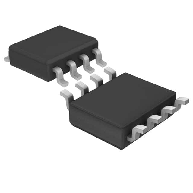
Package: 8-pin SOIC (Small Outline Integrated Circuit)
Essence: The LTC1659IS8#PBF is a high-performance, low-power, 16-bit DAC designed for various applications requiring accurate analog voltage generation.
Packaging/Quantity: The LTC1659IS8#PBF is available in tape and reel packaging with a quantity of 250 units per reel.
Specifications
- Resolution: 16 bits
- Supply Voltage Range: 2.7V to 5.5V
- Output Voltage Range: 0V to Vref
- Integral Nonlinearity (INL): ±1 LSB (Max)
- Differential Nonlinearity (DNL): ±1 LSB (Max)
- Power Consumption: 0.5mW (Typ)
- Operating Temperature Range: -40°C to +85°C
Pin Configuration
The LTC1659IS8#PBF has the following pin configuration:
```
| | --|VDD GND|-- Pin 1: Ground (GND) --|SDI SDO|-- Pin 2: Serial Data Input (SDI) --|SCK CS |-- Pin 3: Serial Clock Input (SCK) --|REF CLR|-- Pin 4: Reference Voltage Input (REF) --|VOUT LDAC|-- Pin 5: Analog Output (VOUT) --|AGND DGND|-- Pin 6: Analog and Digital Ground (AGND/DGND) --|FSYNC SDA|-- Pin 7: Frame Synchronization Input (FSYNC) --|VCC VCC|-- Pin 8: Supply Voltage (VCC) |___________| ```
Functional Features
- High-resolution digital-to-analog conversion
- Serial interface for easy integration with microcontrollers and other digital systems
- Low power consumption for energy-efficient applications
- Wide operating temperature range for versatile usage in various environments
- Reference voltage input for precise analog output generation
- Frame synchronization input for synchronized data transfer
Advantages and Disadvantages
Advantages: - High precision and accuracy - Low power consumption - Compact size - Versatile operating temperature range
Disadvantages: - Limited output voltage range (0V to Vref)
Working Principles
The LTC1659IS8#PBF utilizes a serial interface to receive digital input data, which is then converted into an analog voltage output. The reference voltage input determines the maximum output voltage level. The device operates with high precision and low power consumption, making it suitable for applications requiring accurate analog voltage generation.
Detailed Application Field Plans
The LTC1659IS8#PBF can be used in various applications, including but not limited to: 1. Industrial automation systems 2. Test and measurement equipment 3. Audio signal processing 4. Data acquisition systems 5. Instrumentation and control systems
Detailed and Complete Alternative Models
- AD5662 - 16-Bit, Low Power, Rail-to-Rail Output DAC
- MAX5216 - 16-Bit, Serial, Voltage-Output DAC
- MCP4922 - Dual 12-Bit Digital-to-Analog Converter with SPI Interface
- DAC8562 - Dual, 16-Bit, Ultra-Low Glitch, Voltage Output DAC
These alternative models offer similar functionality and performance to the LTC1659IS8#PBF and can be considered as alternatives based on specific application requirements.
Word count: 380 words
技術ソリューションにおける LTC1659IS8#PBF の適用に関連する 10 件の一般的な質問と回答をリストします。
Sure! Here are 10 common questions and answers related to the application of LTC1659IS8#PBF in technical solutions:
Q: What is LTC1659IS8#PBF? A: LTC1659IS8#PBF is a digital-to-analog converter (DAC) manufactured by Linear Technology (now part of Analog Devices). It is a 16-bit, serial-input, voltage-output DAC.
Q: What is the operating voltage range of LTC1659IS8#PBF? A: The operating voltage range of LTC1659IS8#PBF is typically between 2.7V and 5.5V.
Q: How many bits of resolution does LTC1659IS8#PBF have? A: LTC1659IS8#PBF has a resolution of 16 bits, allowing for precise control over the output voltage.
Q: What is the maximum output voltage range of LTC1659IS8#PBF? A: The maximum output voltage range of LTC1659IS8#PBF is determined by the supply voltage. For example, with a 5V supply, the output voltage can range from 0V to 5V.
Q: Can LTC1659IS8#PBF be used in both single-ended and differential mode? A: Yes, LTC1659IS8#PBF can be used in both single-ended and differential mode, providing flexibility in various applications.
Q: What is the typical settling time of LTC1659IS8#PBF? A: The typical settling time of LTC1659IS8#PBF is around 10µs, ensuring fast response in dynamic applications.
Q: Does LTC1659IS8#PBF have an internal reference voltage? A: No, LTC1659IS8#PBF does not have an internal reference voltage. An external reference voltage is required for accurate operation.
Q: Can LTC1659IS8#PBF be controlled using a microcontroller? A: Yes, LTC1659IS8#PBF can be easily controlled using a microcontroller through its serial interface, making it suitable for digital control applications.
Q: What is the power supply current consumption of LTC1659IS8#PBF? A: The power supply current consumption of LTC1659IS8#PBF is typically around 0.5mA, making it suitable for low-power applications.
Q: Are there any specific application notes or reference designs available for LTC1659IS8#PBF? A: Yes, Analog Devices provides application notes and reference designs on their website that can help in understanding and implementing LTC1659IS8#PBF in various technical solutions.
Please note that the answers provided here are general and may vary depending on the specific datasheet and application requirements. It is always recommended to refer to the official documentation and consult with the manufacturer for accurate information.