

LTC1150CN8#PBF
Product Overview
Category
LTC1150CN8#PBF belongs to the category of integrated circuits (ICs).
Use
This product is commonly used in electronic devices for signal conditioning and amplification.
Characteristics
- LTC1150CN8#PBF is a high-performance operational amplifier.
- It operates with low power consumption, making it suitable for battery-powered applications.
- The device offers high precision and low noise performance.
- It has a wide input voltage range and can operate in both single-supply and dual-supply configurations.
Package
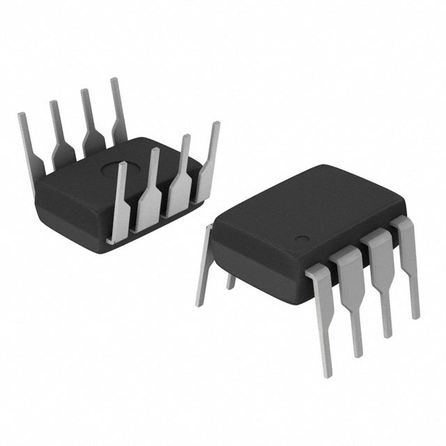
LTC1150CN8#PBF is available in an 8-pin plastic DIP (Dual Inline Package) package.
Essence
The essence of LTC1150CN8#PBF lies in its ability to provide accurate and reliable signal conditioning and amplification in various electronic systems.
Packaging/Quantity
This product is typically sold in reels or tubes, containing a quantity of 50 units per package.
Specifications
- Supply Voltage: ±2.5V to ±18V
- Input Offset Voltage: 150µV (maximum)
- Gain Bandwidth Product: 1.2MHz
- Input Bias Current: 20nA (maximum)
- Output Current: 40mA (maximum)
- Operating Temperature Range: -40°C to 85°C
Detailed Pin Configuration
LTC1150CN8#PBF features the following pin configuration:
- OUT: Output pin
- V+: Positive supply voltage pin
- IN+: Non-inverting input pin
- IN-: Inverting input pin
- V-: Negative supply voltage pin
- NC: No connection
- NC: No connection
- GND: Ground pin
Functional Features
- Low offset voltage and low input bias current ensure accurate signal amplification.
- Rail-to-rail input and output capability allows for maximum dynamic range.
- High gain bandwidth product enables the amplifier to handle a wide range of frequencies.
- The device exhibits excellent linearity and low distortion characteristics.
Advantages and Disadvantages
Advantages
- Low power consumption makes it suitable for battery-powered applications.
- Wide input voltage range allows for versatile use in different systems.
- High precision and low noise performance ensure accurate signal conditioning.
- Can operate in both single-supply and dual-supply configurations.
Disadvantages
- Limited output current may restrict its use in high-power applications.
- The 8-pin package may not be suitable for space-constrained designs.
Working Principles
LTC1150CN8#PBF operates as a voltage amplifier, taking an input signal and amplifying it with high precision. It utilizes internal circuitry to minimize offset voltage and bias currents, ensuring accurate signal reproduction. The amplifier can be configured for various gain settings and is designed to operate within specified supply voltage ranges.
Detailed Application Field Plans
LTC1150CN8#PBF finds application in a wide range of electronic systems, including but not limited to: - Audio amplifiers - Sensor signal conditioning - Data acquisition systems - Instrumentation amplifiers - Active filters
Detailed and Complete Alternative Models
Some alternative models that offer similar functionality to LTC1150CN8#PBF are: - AD8628 - MAX4239 - OPA2277
These alternatives provide comparable performance and can be considered based on specific application requirements.
Word count: 413 words
技術ソリューションにおける LTC1150CN8#PBF の適用に関連する 10 件の一般的な質問と回答をリストします。
Sure! Here are 10 common questions and answers related to the application of LTC1150CN8#PBF in technical solutions:
Q: What is LTC1150CN8#PBF? A: LTC1150CN8#PBF is a high precision, low power, zero-drift operational amplifier manufactured by Linear Technology (now part of Analog Devices).
Q: What are the key features of LTC1150CN8#PBF? A: Some key features include low offset voltage, low input bias current, low quiescent current, wide supply voltage range, and rail-to-rail inputs and outputs.
Q: What are the typical applications of LTC1150CN8#PBF? A: LTC1150CN8#PBF is commonly used in precision instrumentation, sensor signal conditioning, data acquisition systems, and other applications requiring high accuracy amplification.
Q: What is the maximum supply voltage for LTC1150CN8#PBF? A: The maximum supply voltage for LTC1150CN8#PBF is typically ±18V.
Q: What is the input offset voltage of LTC1150CN8#PBF? A: The input offset voltage is typically very low, around 50µV.
Q: Can LTC1150CN8#PBF operate with a single supply voltage? A: Yes, LTC1150CN8#PBF can operate with a single supply voltage as low as 2.7V.
Q: What is the maximum output current of LTC1150CN8#PBF? A: The maximum output current is typically around 20mA.
Q: Does LTC1150CN8#PBF have built-in protection features? A: Yes, LTC1150CN8#PBF has built-in protection against short-circuits and thermal overload.
Q: What is the operating temperature range for LTC1150CN8#PBF? A: The operating temperature range is typically -40°C to +85°C.
Q: Is LTC1150CN8#PBF available in different package options? A: Yes, LTC1150CN8#PBF is available in an 8-pin PDIP package.
Please note that the answers provided here are general and may vary depending on specific datasheet specifications and application requirements.