

LT3420EDD-1#PBF
Product Overview
Category
The LT3420EDD-1#PBF belongs to the category of integrated circuits (ICs) and specifically falls under the power management ICs.
Use
This product is primarily used for power management applications, providing efficient and reliable voltage regulation.
Characteristics
- High efficiency: The LT3420EDD-1#PBF offers high efficiency power conversion, minimizing energy loss.
- Wide input voltage range: It can handle a wide range of input voltages, making it versatile for various applications.
- Low quiescent current: The device has low standby power consumption, ensuring energy efficiency during idle periods.
- Adjustable output voltage: The output voltage can be easily adjusted to meet specific requirements.
Package
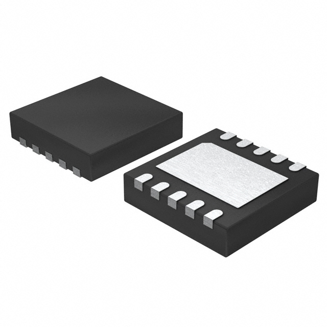
The LT3420EDD-1#PBF is available in a small form factor package, such as a 12-pin DFN (Dual Flat No-Lead) package. This package provides compactness and ease of integration into different systems.
Essence
The essence of LT3420EDD-1#PBF lies in its ability to efficiently regulate voltage, ensuring stable and reliable power supply for electronic devices.
Packaging/Quantity
The product is typically supplied in reels or tubes, depending on the manufacturer's packaging standards. The quantity per reel or tube may vary, but it is commonly available in quantities suitable for both prototyping and mass production.
Specifications
- Input Voltage Range: 2.5V - 20V
- Output Voltage Range: 0.8V - 18V
- Maximum Output Current: 3A
- Switching Frequency: 1MHz
- Quiescent Current: 50µA
- Operating Temperature Range: -40°C to 125°C
Detailed Pin Configuration
The LT3420EDD-1#PBF has a 12-pin DFN package with the following pin configuration:
- VIN: Input voltage pin
- GND: Ground reference pin
- SW: Switching node pin
- FB: Feedback pin for output voltage regulation
- SS: Soft-start capacitor pin
- EN: Enable pin for turning the device on/off
- VOUT: Output voltage pin
- PGND: Power ground pin
- BST: Boost capacitor connection pin
- LX: Inductor connection pin
- NC: No connection pin
- NC: No connection pin
Functional Features
- Wide input voltage range allows compatibility with various power sources.
- Adjustable output voltage enables customization according to specific requirements.
- High efficiency power conversion minimizes energy loss and maximizes battery life.
- Low quiescent current ensures energy efficiency during standby or idle periods.
- Soft-start feature prevents excessive inrush current during startup, protecting the system components.
Advantages and Disadvantages
Advantages
- High efficiency power conversion
- Wide input voltage range
- Adjustable output voltage
- Compact form factor
- Low quiescent current
Disadvantages
- Limited maximum output current (3A)
- Requires external components for operation
Working Principles
The LT3420EDD-1#PBF operates as a step-up (boost) DC-DC converter. It takes an input voltage within the specified range and boosts it to a higher output voltage. The device utilizes a switching regulator topology to efficiently convert the input voltage to the desired output voltage. It employs pulse-width modulation (PWM) techniques to regulate the output voltage accurately.
Detailed Application Field Plans
The LT3420EDD-1#PBF finds applications in various fields, including but not limited to: - Portable electronic devices - Battery-powered systems - Industrial automation - Automotive electronics - Telecommunications equipment
Detailed and Complete Alternative Models
- LT3420EDD#PBF: Similar to LT3420EDD-1#PBF, but without the extended temperature range (-40°C to 125°C).
- LT3420IDD#PBF: A variant with an adjustable current limit feature.
- LT3420EMS8E#PBF: An alternative model in an 8-pin MSOP package.
These alternative models offer similar functionality and characteristics, providing flexibility for different design requirements.
Word count: 566 words
技術ソリューションにおける LT3420EDD-1#PBF の適用に関連する 10 件の一般的な質問と回答をリストします。
Sure! Here are 10 common questions and answers related to the application of LT3420EDD-1#PBF in technical solutions:
Q1: What is the LT3420EDD-1#PBF? A1: The LT3420EDD-1#PBF is a high voltage, low quiescent current step-up DC/DC converter designed for battery-powered applications.
Q2: What is the input voltage range of the LT3420EDD-1#PBF? A2: The input voltage range of the LT3420EDD-1#PBF is from 2.5V to 20V.
Q3: What is the output voltage range of the LT3420EDD-1#PBF? A3: The output voltage range of the LT3420EDD-1#PBF is from 4V to 34V.
Q4: What is the maximum output current of the LT3420EDD-1#PBF? A4: The maximum output current of the LT3420EDD-1#PBF is 1.5A.
Q5: What is the efficiency of the LT3420EDD-1#PBF? A5: The efficiency of the LT3420EDD-1#PBF can reach up to 92%.
Q6: Can the LT3420EDD-1#PBF be used in automotive applications? A6: Yes, the LT3420EDD-1#PBF is suitable for automotive applications as it can operate over a wide temperature range (-40°C to 125°C).
Q7: Does the LT3420EDD-1#PBF have built-in protection features? A7: Yes, the LT3420EDD-1#PBF includes features like overvoltage protection, current limit protection, and thermal shutdown.
Q8: Can the LT3420EDD-1#PBF be used in battery charging applications? A8: Yes, the LT3420EDD-1#PBF can be used for battery charging applications as it supports constant voltage and constant current modes.
Q9: What type of package does the LT3420EDD-1#PBF come in? A9: The LT3420EDD-1#PBF is available in a 10-lead DFN (3mm x 3mm) package.
Q10: Are there any evaluation boards or reference designs available for the LT3420EDD-1#PBF? A10: Yes, Linear Technology (now part of Analog Devices) provides evaluation boards and reference designs for the LT3420EDD-1#PBF to help with its application and development.
Please note that these answers are general and may vary depending on specific application requirements. It's always recommended to refer to the datasheet and consult with the manufacturer for detailed information.