

LT1712CGN#PBF
Product Overview
Category: Integrated Circuit (IC)
Use: The LT1712CGN#PBF is a high-speed operational amplifier designed for use in various electronic applications. It provides excellent performance and versatility, making it suitable for a wide range of uses.
Characteristics: - High-speed operation - Low input offset voltage - Low input bias current - Wide supply voltage range - Rail-to-rail output swing - Low power consumption
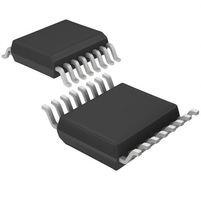
Package: The LT1712CGN#PBF comes in a compact 16-pin SSOP package, which ensures easy integration into circuit designs.
Essence: This IC is an essential component in electronic circuits that require high-speed amplification and precision signal processing.
Packaging/Quantity: The LT1712CGN#PBF is typically sold in reels containing a quantity of 250 units per reel.
Specifications
- Supply Voltage Range: ±2.5V to ±15V
- Input Offset Voltage: 1.5mV (maximum)
- Input Bias Current: 10nA (maximum)
- Gain Bandwidth Product: 100MHz (typical)
- Slew Rate: 50V/µs (typical)
- Quiescent Current: 6mA (typical)
Detailed Pin Configuration
The LT1712CGN#PBF features a 16-pin SSOP package with the following pin configuration:
- OUT-
- V+
- IN+
- IN-
- V-
- NC
- NC
- NC
- NC
- NC
- NC
- NC
- NC
- NC
- NC
- OUT+
Functional Features
- High-speed amplification: The LT1712CGN#PBF offers a wide gain bandwidth product and fast slew rate, enabling it to amplify high-frequency signals accurately.
- Low input offset voltage: This IC has a low input offset voltage, ensuring minimal error in signal amplification.
- Rail-to-rail output swing: The LT1712CGN#PBF provides a wide output voltage range, allowing it to handle signals close to the supply rails.
- Low power consumption: With its low quiescent current, this IC minimizes power consumption, making it suitable for battery-powered applications.
Advantages and Disadvantages
Advantages: - High-speed operation - Low input offset voltage - Wide supply voltage range - Rail-to-rail output swing - Low power consumption
Disadvantages: - Limited pin configuration options - Relatively small package size
Working Principles
The LT1712CGN#PBF operates as a voltage amplifier by amplifying the difference between the IN+ and IN- inputs. It utilizes internal circuitry to provide high-speed amplification while maintaining low input offset voltage and bias current. The rail-to-rail output swing allows it to accurately reproduce amplified signals across a wide range of voltages.
Detailed Application Field Plans
The LT1712CGN#PBF finds applications in various fields, including: 1. Audio amplification systems 2. Communication equipment 3. Test and measurement instruments 4. Data acquisition systems 5. Industrial control systems
Detailed and Complete Alternative Models
- LT1712CGN#TRPBF
- LT1712IGN#PBF
- LT1712IGN#TRPBF
- LT1712IS8#PBF
- LT1712IS8#TRPBF
These alternative models offer similar functionality and performance to the LT1712CGN#PBF, providing flexibility in choosing the most suitable option for specific applications.
Word count: 346 words
技術ソリューションにおける LT1712CGN#PBF の適用に関連する 10 件の一般的な質問と回答をリストします。
Sure! Here are 10 common questions and answers related to the application of LT1712CGN#PBF in technical solutions:
Q: What is LT1712CGN#PBF? A: LT1712CGN#PBF is a specific model number for a high-speed operational amplifier manufactured by Linear Technology (now part of Analog Devices).
Q: What are the key features of LT1712CGN#PBF? A: Some key features of LT1712CGN#PBF include a wide bandwidth, low input bias current, low input offset voltage, and high slew rate.
Q: What are the typical applications of LT1712CGN#PBF? A: LT1712CGN#PBF is commonly used in applications such as active filters, data acquisition systems, medical instrumentation, and high-speed signal processing.
Q: What is the supply voltage range for LT1712CGN#PBF? A: The supply voltage range for LT1712CGN#PBF is typically between ±5V and ±15V.
Q: What is the input voltage range of LT1712CGN#PBF? A: The input voltage range of LT1712CGN#PBF typically extends from the negative supply voltage to the positive supply voltage.
Q: What is the output voltage swing of LT1712CGN#PBF? A: The output voltage swing of LT1712CGN#PBF is typically close to the supply voltage rails.
Q: Does LT1712CGN#PBF require external compensation? A: No, LT1712CGN#PBF is internally compensated and does not require any external components for stability.
Q: What is the maximum operating temperature for LT1712CGN#PBF? A: The maximum operating temperature for LT1712CGN#PBF is typically around 125°C.
Q: Can LT1712CGN#PBF operate with a single supply voltage? A: Yes, LT1712CGN#PBF can be operated with a single supply voltage by connecting the negative supply pin to ground.
Q: Is LT1712CGN#PBF available in different package options? A: Yes, LT1712CGN#PBF is available in various package options, including the 16-pin SSOP and DIP packages.
Please note that the answers provided here are general and may vary depending on specific datasheet specifications or application requirements.