

LFXP2-8E-7MN132C
Product Overview
Category
LFXP2-8E-7MN132C belongs to the category of Field-Programmable Gate Arrays (FPGAs).
Use
This product is primarily used in digital circuit design and prototyping. FPGAs provide a flexible platform for implementing complex logic functions, making them suitable for a wide range of applications.
Characteristics
- High flexibility: FPGAs can be reprogrammed to perform different functions, allowing for rapid prototyping and design iterations.
- Parallel processing: FPGAs can execute multiple tasks simultaneously, enabling high-performance computing.
- Customizability: Users can configure the FPGA to meet their specific requirements by programming the internal logic elements.
- Scalability: FPGAs offer various sizes and configurations to accommodate different project needs.
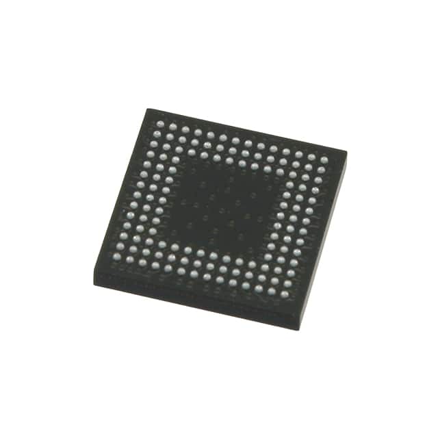
Package
The LFXP2-8E-7MN132C comes in a compact package that ensures easy integration into electronic systems. It is designed to be mounted on a printed circuit board (PCB) using surface mount technology (SMT).
Essence
The essence of LFXP2-8E-7MN132C lies in its ability to provide a versatile and customizable hardware platform for digital circuit implementation.
Packaging/Quantity
The LFXP2-8E-7MN132C is typically packaged in reels or trays, with each reel containing a specified quantity of units. The exact packaging and quantity may vary depending on the supplier.
Specifications
- Device family: LatticeXP2
- Logic cells: 8,000
- Look-up tables (LUTs): 8,000
- Flip-flops: 16,000
- Maximum user I/Os: 132
- Operating voltage: 1.2V
- Speed grade: -7
- Package type: MN132
Detailed Pin Configuration
The LFXP2-8E-7MN132C has a total of 132 pins, each serving a specific purpose in the FPGA's operation. The pin configuration is as follows:
(Pin Number) - (Pin Name) - (Function)
1 - GND - Ground 2 - VCCINT - Internal core voltage supply 3 - VCCAUX - Auxiliary voltage supply 4 - IOB0 - User I/O buffer 5 - IOB1 - User I/O buffer ... 132 - IOB_131 - User I/O buffer
Please refer to the product datasheet for a complete pin configuration diagram.
Functional Features
- High-speed performance: The LFXP2-8E-7MN132C offers fast signal processing capabilities, making it suitable for applications requiring real-time data processing.
- Low power consumption: This FPGA is designed to operate efficiently with low power requirements, enabling energy-efficient designs.
- On-chip memory: The device includes embedded memory blocks that can be used for storing data or implementing complex algorithms.
- Built-in security features: The LFXP2-8E-7MN132C incorporates security mechanisms to protect sensitive information and prevent unauthorized access.
Advantages and Disadvantages
Advantages
- Flexibility: FPGAs allow for rapid prototyping and design iterations, reducing time-to-market.
- Customizability: Users can tailor the FPGA's functionality to their specific application requirements.
- Parallel processing: FPGAs can execute multiple tasks simultaneously, enabling high-performance computing.
- Scalability: FPGAs are available in various sizes and configurations, accommodating different project needs.
Disadvantages
- Complexity: Designing and programming FPGAs require specialized knowledge and expertise.
- Cost: FPGAs can be more expensive than other integrated circuits due to their versatility and customization options.
- Power consumption: FPGAs may consume more power compared to application-specific integrated circuits (ASICs) for certain applications.
Working Principles
The LFXP2-8E-7MN132C operates based on the principles of reconfigurable logic. It consists of an array of configurable logic blocks (CLBs) interconnected by programmable routing resources. Users can program the CLBs to implement desired logic functions, creating custom digital circuits within the FPGA.
During operation, the FPGA's configuration memory is loaded with a bitstream that defines the desired circuit functionality. The internal interconnections are established according to this configuration, allowing the FPGA to perform the specified operations.
Detailed Application Field Plans
The LFXP2-8E-7MN132C finds applications in various fields, including:
- Communications: Used in wireless base stations, network routers, and communication infrastructure equipment.
- Industrial automation: Employed in control systems, robotics, and process automation.
- Automotive electronics: Utilized in vehicle control units, driver assistance systems, and infotainment systems.
- Aerospace and defense: Applied in
技術ソリューションにおける LFXP2-8E-7MN132C の適用に関連する 10 件の一般的な質問と回答をリストします。
Sure! Here are 10 common questions and answers related to the application of LFXP2-8E-7MN132C in technical solutions:
Q: What is LFXP2-8E-7MN132C? A: LFXP2-8E-7MN132C is a field-programmable gate array (FPGA) manufactured by Lattice Semiconductor.
Q: What are the key features of LFXP2-8E-7MN132C? A: Some key features of LFXP2-8E-7MN132C include 8,000 Look-Up Tables (LUTs), 132 user I/O pins, and support for various I/O standards.
Q: What applications can LFXP2-8E-7MN132C be used for? A: LFXP2-8E-7MN132C can be used in a wide range of applications such as industrial automation, automotive electronics, telecommunications, and consumer electronics.
Q: How can LFXP2-8E-7MN132C be programmed? A: LFXP2-8E-7MN132C can be programmed using hardware description languages (HDLs) like VHDL or Verilog, or through graphical programming tools provided by Lattice Semiconductor.
Q: What is the power supply requirement for LFXP2-8E-7MN132C? A: LFXP2-8E-7MN132C requires a single power supply voltage of 1.2V.
Q: Can LFXP2-8E-7MN132C interface with other devices? A: Yes, LFXP2-8E-7MN132C supports various communication protocols such as SPI, I2C, UART, and GPIO, allowing it to interface with other devices.
Q: What is the maximum operating frequency of LFXP2-8E-7MN132C? A: The maximum operating frequency of LFXP2-8E-7MN132C is typically around 300 MHz, depending on the design and implementation.
Q: Can LFXP2-8E-7MN132C be used for real-time applications? A: Yes, LFXP2-8E-7MN132C can be used for real-time applications as it offers fast logic processing and low-latency I/O capabilities.
Q: Does LFXP2-8E-7MN132C support secure boot or encryption? A: No, LFXP2-8E-7MN132C does not have built-in support for secure boot or encryption. Additional security measures may need to be implemented externally.
Q: Where can I find more information about LFXP2-8E-7MN132C? A: You can find more detailed information about LFXP2-8E-7MN132C in the datasheet provided by Lattice Semiconductor or on their official website.