

LFXP2-40E-6FN672I
Product Overview
Category
The LFXP2-40E-6FN672I belongs to the category of Field Programmable Gate Arrays (FPGAs).
Use
This FPGA is commonly used in electronic circuits for various applications, including digital signal processing, telecommunications, automotive electronics, and industrial automation.
Characteristics
- High-performance programmable logic device
- Low power consumption
- Flexible and reconfigurable design
- Large number of input/output pins
- High-speed data processing capabilities
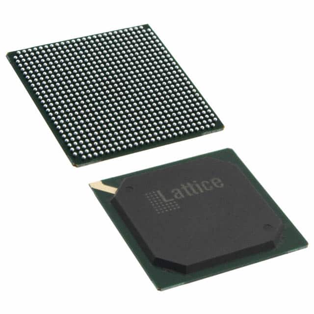
Package
The LFXP2-40E-6FN672I comes in a compact and durable package, ensuring easy integration into electronic systems.
Essence
The essence of this FPGA lies in its ability to provide a customizable hardware platform that can be programmed to perform specific functions as required by the application.
Packaging/Quantity
The LFXP2-40E-6FN672I is typically packaged individually and is available in varying quantities depending on the manufacturer or supplier.
Specifications
- Device Type: Field Programmable Gate Array (FPGA)
- Model: LFXP2-40E-6FN672I
- Logic Cells: 40,000
- Number of I/O Pins: 672
- Operating Voltage: 1.2V
- Maximum Frequency: 500 MHz
- Configuration Memory: Flash-based
Detailed Pin Configuration
The LFXP2-40E-6FN672I has a total of 672 pins, which are divided into different categories based on their functionality. The pin configuration includes:
- Power supply pins
- Ground pins
- Input pins
- Output pins
- Clock pins
- Configuration pins
- Special function pins
For a detailed pin configuration diagram, please refer to the datasheet provided by the manufacturer.
Functional Features
- High-speed data processing capabilities
- Configurable logic blocks for implementing complex functions
- Dedicated hardware resources for arithmetic operations
- On-chip memory for storing intermediate results
- Built-in support for various communication protocols
- Flexible clock management and synchronization options
Advantages and Disadvantages
Advantages
- Flexibility and reconfigurability allow for quick prototyping and design iterations
- High-performance computing capabilities enable complex algorithms to be implemented efficiently
- Large number of I/O pins provide extensive connectivity options
- Low power consumption makes it suitable for battery-powered applications
Disadvantages
- Steep learning curve for beginners due to the complexity of FPGA programming
- Higher cost compared to other programmable logic devices
- Limited availability of open-source tools and libraries for FPGA development
Working Principles
The LFXP2-40E-6FN672I operates based on the principles of digital logic. It consists of configurable logic blocks, interconnects, and dedicated hardware resources. The device can be programmed using a Hardware Description Language (HDL) such as VHDL or Verilog. Once programmed, the FPGA executes the desired logic functions by routing signals through the configurable logic blocks and interconnects.
Detailed Application Field Plans
The LFXP2-40E-6FN672I finds applications in various fields, including:
- Digital Signal Processing: Used for implementing complex algorithms in audio and video processing systems.
- Telecommunications: Employed in network routers, switches, and base stations for high-speed data processing.
- Automotive Electronics: Integrated into automotive control systems for functions like engine management and driver assistance.
- Industrial Automation: Utilized in programmable logic controllers (PLCs) for process control and automation tasks.
Detailed and Complete Alternative Models
- Xilinx Spartan-6 XC6SLX150T: Offers similar performance and features with a larger logic capacity.
- Intel Cyclone V EP4CE115F29C7: Provides comparable capabilities with a different architecture and toolchain.
- Lattice ECP5-85: Offers lower power consumption and smaller form factor with similar functionality.
These alternative models can be considered based on specific project requirements and design constraints.
Word count: 530 words
技術ソリューションにおける LFXP2-40E-6FN672I の適用に関連する 10 件の一般的な質問と回答をリストします。
Sure! Here are 10 common questions and answers related to the application of LFXP2-40E-6FN672I in technical solutions:
Q: What is LFXP2-40E-6FN672I? A: LFXP2-40E-6FN672I is a field-programmable gate array (FPGA) manufactured by Lattice Semiconductor.
Q: What are the key features of LFXP2-40E-6FN672I? A: Some key features include 40,960 logic cells, 672-pin fine pitch ball grid array (FBGA) package, low power consumption, and high-speed performance.
Q: What are the typical applications of LFXP2-40E-6FN672I? A: LFXP2-40E-6FN672I is commonly used in various technical solutions such as industrial automation, telecommunications, automotive electronics, medical devices, and consumer electronics.
Q: How can LFXP2-40E-6FN672I be programmed? A: LFXP2-40E-6FN672I can be programmed using hardware description languages (HDLs) like VHDL or Verilog, or through graphical programming tools provided by Lattice Semiconductor.
Q: What is the maximum operating frequency of LFXP2-40E-6FN672I? A: The maximum operating frequency of LFXP2-40E-6FN672I is typically around 400 MHz, depending on the design and implementation.
Q: Can LFXP2-40E-6FN672I interface with other components or devices? A: Yes, LFXP2-40E-6FN672I supports various standard interfaces such as SPI, I2C, UART, and GPIOs, allowing it to communicate with other components or devices in a system.
Q: What is the power supply requirement for LFXP2-40E-6FN672I? A: LFXP2-40E-6FN672I requires a single 1.2V power supply for its core logic, and additional power supplies for I/O banks if needed.
Q: Can LFXP2-40E-6FN672I be reprogrammed after deployment? A: Yes, LFXP2-40E-6FN672I is a field-programmable device, which means it can be reprogrammed even after it has been deployed in a system.
Q: Are there any development tools available for LFXP2-40E-6FN672I? A: Yes, Lattice Semiconductor provides development tools like Lattice Diamond or Lattice Radiant software suites for designing, simulating, and programming LFXP2-40E-6FN672I.
Q: Where can I find more information about LFXP2-40E-6FN672I? A: You can find more detailed information about LFXP2-40E-6FN672I, including datasheets, application notes, and reference designs, on the official website of Lattice Semiconductor or by contacting their technical support team.