

LFXP2-40E-6F672C
Product Overview
Category: Programmable Logic Device (PLD)
Use: The LFXP2-40E-6F672C is a high-performance PLD designed for various digital logic applications. It offers flexible programmability and advanced features, making it suitable for a wide range of electronic systems.
Characteristics: - High-speed operation - Low power consumption - Large capacity - Small form factor - Easy integration with other components
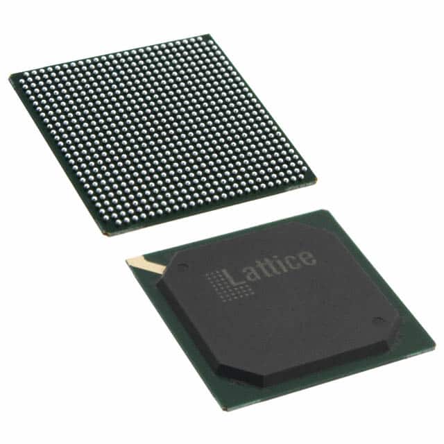
Package: The LFXP2-40E-6F672C comes in a compact and durable package, ensuring protection during handling and installation. The package is designed to facilitate easy soldering onto printed circuit boards.
Essence: The essence of the LFXP2-40E-6F672C lies in its ability to provide customizable logic functions, allowing designers to implement complex digital circuits efficiently.
Packaging/Quantity: The LFXP2-40E-6F672C is typically packaged individually and is available in various quantities depending on the manufacturer's specifications.
Specifications
- Logic Cells: 40,000
- Flip-Flops: 6,672
- Maximum Frequency: 400 MHz
- I/O Pins: 672
- Operating Voltage: 1.2V
- Package Type: FineLine BGA
- Temperature Range: -40°C to +85°C
Detailed Pin Configuration
The LFXP2-40E-6F672C has a well-defined pin configuration that allows for easy integration into electronic systems. Here are some key pins:
- VCCIO: Power supply voltage for input/output buffers.
- GND: Ground reference.
- JTAGTMS, JTAGTCK, JTAGTDI, JTAGTDO: Pins used for Joint Test Action Group (JTAG) boundary scan testing.
- I/O Pins: Multiple pins for input and output signals.
For a complete pin configuration diagram, please refer to the manufacturer's datasheet.
Functional Features
- High-speed performance: The LFXP2-40E-6F672C operates at a maximum frequency of 400 MHz, enabling rapid data processing.
- Flexible programmability: It offers a wide range of logic functions that can be customized to meet specific application requirements.
- Low power consumption: The device is designed to minimize power consumption, making it suitable for battery-powered applications.
- Large capacity: With 40,000 logic cells and 6,672 flip-flops, the PLD can handle complex digital designs efficiently.
- Easy integration: The LFXP2-40E-6F672C can be easily integrated into existing electronic systems, thanks to its well-defined pin configuration.
Advantages and Disadvantages
Advantages: - Versatile programmability allows for customization. - High-speed operation enables efficient data processing. - Low power consumption extends battery life in portable devices. - Compact form factor saves space on printed circuit boards. - Easy integration with other components simplifies system design.
Disadvantages: - Limited availability of alternative models from different manufacturers. - Higher cost compared to simpler logic devices for less complex applications. - Steeper learning curve for designers unfamiliar with programmable logic devices.
Working Principles
The LFXP2-40E-6F672C utilizes a combination of configurable logic blocks, interconnect resources, and input/output buffers to implement custom digital circuits. These circuits are programmed using hardware description languages or specialized software tools provided by the manufacturer. The PLD's internal architecture allows for the creation of complex logic functions by configuring the interconnections between logic elements.
Detailed Application Field Plans
The LFXP2-40E-6F672C finds applications in various fields, including:
- Embedded Systems: It can be used to implement control and communication functions in embedded systems such as industrial automation, robotics, and automotive electronics.
- Telecommunications: The PLD's high-speed operation makes it suitable for applications in telecommunications infrastructure, including network switches and routers.
- Consumer Electronics: It can be utilized in consumer electronic devices like gaming consoles, smart TVs, and home automation systems to enable advanced functionality.
- Medical Devices: The LFXP2-40E-6F672C can be integrated into medical devices for signal processing, data acquisition, and control purposes.
Detailed and Complete Alternative Models
While the LFXP2-40E-6F672C offers excellent features, there are alternative models available from different manufacturers that cater to similar requirements. Some notable alternatives include:
- Xilinx Spartan-6 FPGA series
- Altera Cyclone IV E FPGA series
- Microchip PolarFire FPGA series
These alternative models provide a range of options in terms of capacity, performance, and cost, allowing designers to
技術ソリューションにおける LFXP2-40E-6F672C の適用に関連する 10 件の一般的な質問と回答をリストします。
Sure! Here are 10 common questions and answers related to the application of LFXP2-40E-6F672C in technical solutions:
Q: What is the LFXP2-40E-6F672C? A: The LFXP2-40E-6F672C is a field-programmable gate array (FPGA) manufactured by Lattice Semiconductor.
Q: What are the key features of the LFXP2-40E-6F672C? A: The key features include 40,960 logic cells, 672 I/O pins, 6 input/output banks, and support for various communication protocols.
Q: What are some typical applications of the LFXP2-40E-6F672C? A: The LFXP2-40E-6F672C is commonly used in industrial automation, telecommunications, automotive electronics, and medical devices.
Q: How can I program the LFXP2-40E-6F672C? A: You can program the FPGA using Lattice Diamond or Lattice Radiant software tools provided by Lattice Semiconductor.
Q: Can I use the LFXP2-40E-6F672C for high-speed data processing? A: Yes, the LFXP2-40E-6F672C supports high-speed interfaces like DDR3/DDR4 memory controllers and PCIe.
Q: Does the LFXP2-40E-6F672C have built-in security features? A: Yes, it offers advanced security features such as bitstream encryption and authentication to protect your designs.
Q: Can I interface the LFXP2-40E-6F672C with other components or microcontrollers? A: Yes, the FPGA has multiple I/O banks that can be used to interface with other components or microcontrollers.
Q: What is the power supply requirement for the LFXP2-40E-6F672C? A: The FPGA requires a 1.2V core voltage and a 3.3V I/O voltage for proper operation.
Q: Are there any development boards available for the LFXP2-40E-6F672C? A: Yes, Lattice Semiconductor provides development boards like the ECP5 Versa Evaluation Board for prototyping and testing.
Q: Where can I find technical documentation and support for the LFXP2-40E-6F672C? A: You can find technical documentation, application notes, and support resources on the Lattice Semiconductor website.