

LFEC1E-3Q208I
Product Overview
Category
LFEC1E-3Q208I belongs to the category of Field Programmable Gate Arrays (FPGAs).
Use
This product is primarily used in digital logic circuits for various applications such as telecommunications, automotive, consumer electronics, and industrial automation.
Characteristics
- High-performance programmable logic device
- Offers flexibility and reconfigurability
- Provides a large number of configurable logic blocks and input/output pins
- Supports complex digital designs
- Enables rapid prototyping and development cycles
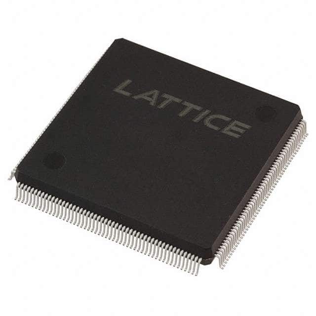
Package
LFEC1E-3Q208I comes in a compact and durable package designed to withstand harsh operating conditions. The package ensures reliable performance and easy integration into electronic systems.
Essence
The essence of LFEC1E-3Q208I lies in its ability to provide a versatile platform for implementing custom digital logic designs. It allows users to create complex circuits tailored to their specific requirements.
Packaging/Quantity
LFEC1E-3Q208I is typically packaged individually and is available in various quantities depending on the user's needs.
Specifications
- Logic Elements: 1,500
- Flip-Flops: 6,000
- Embedded Memory: 2,400 Kbits
- Maximum Frequency: 300 MHz
- I/O Pins: 208
- Voltage Range: 1.2V - 1.5V
- Operating Temperature: -40°C to 100°C
Detailed Pin Configuration
LFEC1E-3Q208I features a comprehensive pin configuration that enables seamless integration into different circuit designs. The detailed pin configuration is as follows:
- Pin 1: VCCIO
- Pin 2: GND
- Pin 3: IOB_0
- Pin 4: IOB_1
- ...
- Pin 208: IOB_206
Functional Features
High-Speed Performance
LFEC1E-3Q208I offers high-speed performance, allowing for efficient execution of complex digital logic designs. It can handle demanding applications that require rapid data processing and real-time operations.
Reconfigurability
One of the key features of LFEC1E-3Q208I is its reconfigurability. Users can modify the circuit design by reprogramming the FPGA, eliminating the need for hardware changes. This flexibility enables quick iterations and modifications during the development process.
Versatility
With a large number of configurable logic blocks and input/output pins, LFEC1E-3Q208I provides versatility in implementing various digital logic circuits. It supports a wide range of applications, making it suitable for diverse industries.
Advantages and Disadvantages
Advantages
- Flexibility in designing custom digital logic circuits
- Rapid prototyping and development cycles
- High-performance capabilities
- Reconfigurable nature allows for easy modifications
Disadvantages
- Steeper learning curve compared to traditional fixed-function integrated circuits
- Higher power consumption compared to dedicated application-specific integrated circuits (ASICs)
- Relatively higher cost per unit compared to mass-produced ASICs
Working Principles
LFEC1E-3Q208I operates based on the principles of field-programmable gate arrays. It consists of configurable logic blocks interconnected through programmable routing resources. These logic blocks can be programmed to perform specific functions, enabling the implementation of complex digital circuits.
The device utilizes look-up tables, flip-flops, and other components to execute logical operations and store data. The configuration of these elements can be modified by loading a bitstream into the FPGA, allowing for customization and adaptability.
Detailed Application Field Plans
LFEC1E-3Q208I finds applications in various fields, including:
- Telecommunications: Used in network routers, switches, and communication infrastructure for high-speed data processing.
- Automotive: Employed in automotive electronics for functions like engine control, advanced driver-assistance systems (ADAS), and infotainment systems.
- Consumer Electronics: Integrated into devices such as smartphones, tablets, and gaming consoles to enable complex functionalities and enhance performance.
- Industrial Automation: Utilized in industrial control systems, robotics, and factory automation for real-time monitoring and control.
Detailed and Complete Alternative Models
- LFEC1E-5TN144C
- LFEC1E-4FN256I
- LFEC1E-6FTN256C
- LFEC1E-7TN100I
- LFEC1E-8FN256C
These alternative models offer similar features and capabilities to LFEC1E-3Q208I, providing users with a range of options based on their specific requirements.
In conclusion, LFEC1E-3Q208I is a high-performance FPGA that offers flexibility, reconfigurability, and versatility in implementing custom digital logic circuits.
技術ソリューションにおける LFEC1E-3Q208I の適用に関連する 10 件の一般的な質問と回答をリストします。
Sure! Here are 10 common questions and answers related to the application of LFEC1E-3Q208I in technical solutions:
1. What is LFEC1E-3Q208I? - LFEC1E-3Q208I is a specific model of Field-Programmable Gate Array (FPGA) manufactured by a company called Lattice Semiconductor.
2. What are the key features of LFEC1E-3Q208I? - LFEC1E-3Q208I offers high-performance logic fabric, low power consumption, and a large number of programmable logic cells. It also supports various I/O standards and has built-in memory blocks.
3. In what applications can LFEC1E-3Q208I be used? - LFEC1E-3Q208I can be used in a wide range of applications such as telecommunications, industrial automation, automotive electronics, medical devices, and aerospace systems.
4. How does LFEC1E-3Q208I help in technical solutions? - LFEC1E-3Q208I provides a flexible and customizable hardware platform that allows engineers to implement complex digital designs and algorithms efficiently. It enables rapid prototyping, system integration, and performance optimization.
5. What programming languages can be used with LFEC1E-3Q208I? - LFEC1E-3Q208I can be programmed using Hardware Description Languages (HDLs) such as VHDL or Verilog. Designers can write code to describe the desired functionality and then synthesize it into a configuration file for the FPGA.
6. Can LFEC1E-3Q208I interface with other components or devices? - Yes, LFEC1E-3Q208I supports various communication protocols and interfaces like SPI, I2C, UART, and Ethernet. It can easily interface with other components or devices in a system.
7. How does LFEC1E-3Q208I handle power consumption? - LFEC1E-3Q208I is designed to be power-efficient. It offers multiple power-saving features like clock gating, dynamic voltage scaling, and low-power standby modes to minimize power consumption when not actively processing data.
8. Can LFEC1E-3Q208I be reprogrammed after deployment? - Yes, LFEC1E-3Q208I is a field-programmable device, which means it can be reprogrammed even after it has been deployed in a system. This allows for flexibility and the ability to update or modify the functionality as needed.
9. Are there any development tools available for LFEC1E-3Q208I? - Yes, Lattice Semiconductor provides a suite of development tools called Lattice Diamond that includes design entry, synthesis, simulation, and programming tools specifically tailored for their FPGAs, including LFEC1E-3Q208I.
10. Where can I find more information about LFEC1E-3Q208I? - You can find more detailed information about LFEC1E-3Q208I on the official website of Lattice Semiconductor. They provide datasheets, application notes, reference designs, and technical support resources for their products.