

商品詳細は仕様をご覧ください。
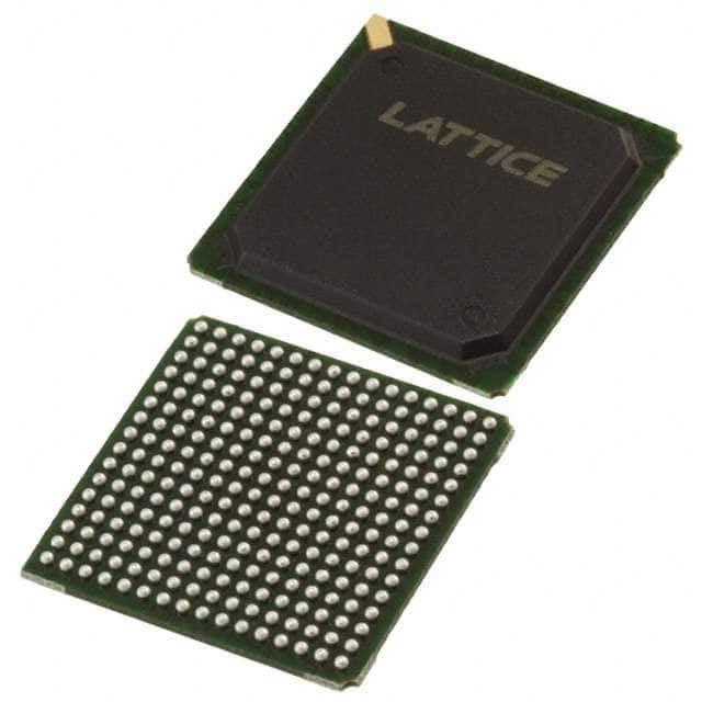
LFEC15E-3F256C
Product Overview
Category
The LFEC15E-3F256C belongs to the category of Field Programmable Gate Arrays (FPGAs).
Use
This FPGA is commonly used in electronic circuits for digital logic implementation, prototyping, and system integration.
Characteristics
- High flexibility: The LFEC15E-3F256C offers a high degree of flexibility due to its reprogrammable nature.
- Customizability: It allows users to design and implement their own digital logic circuits.
- Scalability: The FPGA can be easily scaled up or down depending on the complexity of the desired circuit.
- Fast prototyping: It enables rapid prototyping of digital systems, reducing development time.
Package
The LFEC15E-3F256C comes in a compact package that ensures easy integration into electronic circuits. The package is designed to provide protection against environmental factors such as moisture and dust.
Essence
The essence of the LFEC15E-3F256C lies in its ability to perform complex digital logic functions through programmable interconnections and configurable logic blocks.
Packaging/Quantity
The LFEC15E-3F256C is typically packaged individually and is available in various quantities depending on the manufacturer's specifications.
Specifications
- Logic Elements: 15,000
- Flip-Flops: 256
- Block RAM: 3,000 Kbits
- Maximum Frequency: 400 MHz
- I/O Pins: 256
- Voltage Range: 1.2V - 3.3V
- Operating Temperature: -40°C to 100°C
Detailed Pin Configuration
The LFEC15E-3F256C has a total of 256 I/O pins, each serving a specific purpose in the digital circuit. The pin configuration varies depending on the specific application and user requirements. Please refer to the manufacturer's datasheet for detailed pin configuration information.
Functional Features
- High-speed performance: The LFEC15E-3F256C offers high-speed operation, making it suitable for applications that require quick response times.
- Low power consumption: It is designed to minimize power consumption, making it energy-efficient and suitable for battery-powered devices.
- Embedded memory: The FPGA includes a significant amount of embedded memory, allowing for efficient data storage and retrieval.
- Configurable I/O standards: It supports various I/O standards, enabling seamless integration with different electronic components.
Advantages and Disadvantages
Advantages
- Flexibility: The reprogrammable nature of FPGAs allows for easy modifications and updates to the digital logic design.
- Rapid prototyping: FPGAs enable quick development and testing of digital systems, reducing time-to-market.
- Customizability: Users can implement their own unique digital logic circuits tailored to specific application requirements.
Disadvantages
- Complexity: Designing complex circuits on an FPGA requires expertise in digital logic design and programming.
- Cost: FPGAs can be more expensive compared to other integrated circuits due to their advanced features and flexibility.
- Power consumption: While efforts have been made to reduce power consumption, FPGAs still consume more power compared to dedicated ASICs (Application-Specific Integrated Circuits).
Working Principles
The LFEC15E-3F256C operates based on the principles of configurable logic blocks (CLBs) and programmable interconnects. CLBs consist of look-up tables (LUTs), flip-flops, and multiplexers, which can be programmed to perform various logic functions. The programmable interconnects allow users to establish connections between different CLBs, enabling the creation of complex digital circuits.
Detailed Application Field Plans
The LFEC15E-3F256C finds applications in various fields, including: - Telecommunications: Used in the development of communication systems and network infrastructure. - Aerospace and Defense: Employed in radar systems, avionics, and military-grade electronics. - Industrial Automation: Utilized for control systems, robotics, and process automation. - Medical Devices: Integrated into medical imaging equipment, patient monitoring systems, and diagnostic devices.
Detailed and Complete Alternative Models
- LFEC10E-4FN256C
- LFEC20E-5FN256C
- LFEC25E-6FN256C
- LFEC30E-7FN256C
These alternative models offer similar functionality and performance characteristics to the LFEC15E-3F256C. Users can choose the most suitable model based on their specific requirements and project constraints.
Word count: 609 words
技術ソリューションにおける LFEC15E-3F256C の適用に関連する 10 件の一般的な質問と回答をリストします。
Sure! Here are 10 common questions and answers related to the application of LFEC15E-3F256C in technical solutions:
Q: What is LFEC15E-3F256C? A: LFEC15E-3F256C is a specific model of Field-Programmable Gate Array (FPGA) manufactured by Lattice Semiconductor.
Q: What are the key features of LFEC15E-3F256C? A: LFEC15E-3F256C offers 15,000 Look-Up Tables (LUTs), 256 I/O pins, and supports various advanced technologies like high-speed SERDES, DSP blocks, and embedded memory.
Q: In what applications can LFEC15E-3F256C be used? A: LFEC15E-3F256C can be used in a wide range of applications including telecommunications, industrial automation, automotive electronics, medical devices, and more.
Q: How does LFEC15E-3F256C benefit technical solutions? A: LFEC15E-3F256C provides flexibility and reconfigurability, allowing engineers to implement custom logic functions and algorithms in hardware, resulting in faster and more efficient solutions.
Q: Can LFEC15E-3F256C handle high-speed data transmission? A: Yes, LFEC15E-3F256C supports high-speed Serializers/Deserializers (SERDES) technology, enabling it to handle high-speed data transmission up to several gigabits per second.
Q: Does LFEC15E-3F256C have built-in memory? A: Yes, LFEC15E-3F256C has embedded memory blocks that can be used for storing data or implementing memory-intensive functions.
Q: Can LFEC15E-3F256C interface with other components or devices? A: Yes, LFEC15E-3F256C has a large number of I/O pins that can be used to interface with other components or devices such as sensors, actuators, displays, and communication interfaces.
Q: Is programming LFEC15E-3F256C difficult? A: Programming LFEC15E-3F256C requires knowledge of Hardware Description Languages (HDLs) like VHDL or Verilog. However, there are user-friendly development tools available that simplify the programming process.
Q: Can LFEC15E-3F256C be reprogrammed after deployment? A: Yes, LFEC15E-3F256C is a Field-Programmable device, which means it can be reprogrammed even after it has been deployed in a system, allowing for updates or modifications.
Q: Where can I find more information about LFEC15E-3F256C? A: You can find detailed technical documentation, datasheets, application notes, and support resources on the official website of Lattice Semiconductor or by contacting their customer support.