

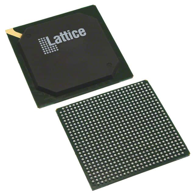
LFE3-70EA-6FN672C
Product Overview
Category
The LFE3-70EA-6FN672C belongs to the category of Field Programmable Gate Arrays (FPGAs).
Use
This FPGA is commonly used in electronic circuits for various applications such as digital signal processing, communication systems, and embedded systems.
Characteristics
- High-performance programmable logic device
- Offers flexibility and reconfigurability
- Provides high-speed data processing capabilities
- Supports complex algorithms and computations
- Enables rapid prototyping and development
Package
The LFE3-70EA-6FN672C comes in a compact and durable package that ensures protection during handling and installation.
Essence
The essence of this FPGA lies in its ability to provide a customizable hardware platform that can be programmed to perform specific functions according to the user's requirements.
Packaging/Quantity
Each package contains one unit of LFE3-70EA-6FN672C FPGA.
Specifications
- Model: LFE3-70EA-6FN672C
- Logic Elements: 70,000
- Number of I/O Pins: 672
- Operating Voltage: 1.2V
- Maximum Frequency: 500 MHz
- Embedded Memory: 4.5 Mb
- Configuration Memory: 8 Mb
- Package Type: BGA (Ball Grid Array)
- Temperature Range: -40°C to +100°C
Detailed Pin Configuration
The LFE3-70EA-6FN672C FPGA has a total of 672 pins, which are divided into different categories:
- Power Supply Pins: These pins provide the necessary voltage levels for the proper functioning of the FPGA.
- Input/Output Pins: These pins are used for interfacing with external devices and circuits.
- Clock Pins: These pins receive clock signals to synchronize the operations of the FPGA.
- Configuration Pins: These pins are used for programming and configuring the FPGA.
For a detailed pin configuration diagram, please refer to the manufacturer's datasheet.
Functional Features
- High-speed data processing capabilities
- Support for various communication protocols
- Flexible and reconfigurable architecture
- Embedded memory for efficient data storage
- Low power consumption
- Built-in security features for protecting intellectual property
Advantages and Disadvantages
Advantages
- Versatile and customizable hardware platform
- Rapid prototyping and development
- High-performance computing capabilities
- Support for complex algorithms and computations
- Reduced time-to-market for electronic products
Disadvantages
- Steep learning curve for beginners
- Higher cost compared to traditional fixed-function integrated circuits
- Limited availability of technical support for specific applications
Working Principles
The LFE3-70EA-6FN672C FPGA operates based on the principles of digital logic. It consists of configurable logic blocks (CLBs), interconnect resources, and embedded memory elements. The CLBs can be programmed to implement various logical functions, while the interconnect resources allow for the routing of signals between different components. The embedded memory elements provide storage for data and instructions.
Upon programming, the FPGA executes the desired functions by manipulating the input signals through the configured logic blocks. The output signals are then routed to the appropriate pins for further processing or interfacing with external devices.
Detailed Application Field Plans
The LFE3-70EA-6FN672C FPGA finds applications in various fields, including:
- Digital Signal Processing: Used for implementing complex algorithms in audio and video processing systems.
- Communication Systems: Enables the development of high-speed data transmission and networking equipment.
- Embedded Systems: Provides a flexible platform for designing and prototyping embedded systems such as IoT devices and industrial control systems.
- Aerospace and Defense: Used in radar systems, avionics, and military communication equipment.
- Scientific Research: Supports data acquisition and processing in scientific experiments and simulations.
Detailed and Complete Alternative Models
- LFE3-35EA-6FN672C: A lower-cost alternative with 35,000 logic elements and similar specifications.
- LFE3-150EA-7FN672C: A higher-performance alternative with 150,000 logic elements and enhanced features.
- LFE3-25EA-8FN672C: A low-power alternative with 25,000 logic elements, suitable for battery-powered applications.
These alternative models provide options based on specific project requirements, budget constraints, and performance needs.
Word count: 610 words
技術ソリューションにおける LFE3-70EA-6FN672C の適用に関連する 10 件の一般的な質問と回答をリストします。
Sure! Here are 10 common questions and answers related to the application of LFE3-70EA-6FN672C in technical solutions:
Q: What is the LFE3-70EA-6FN672C? A: The LFE3-70EA-6FN672C is a field-programmable gate array (FPGA) manufactured by Lattice Semiconductor.
Q: What are the key features of the LFE3-70EA-6FN672C? A: The key features include 70,000 Look-Up Tables (LUTs), 1,080 kilobits of embedded memory, high-speed I/O interfaces, and low power consumption.
Q: In what applications can the LFE3-70EA-6FN672C be used? A: The LFE3-70EA-6FN672C can be used in various applications such as telecommunications, industrial automation, automotive electronics, and medical devices.
Q: How does the LFE3-70EA-6FN672C help in telecommunications applications? A: It can be used for tasks like signal processing, protocol conversion, and data encryption/decryption in telecommunication systems.
Q: Can the LFE3-70EA-6FN672C be used in industrial automation? A: Yes, it can be used for tasks like motor control, sensor interfacing, and real-time monitoring in industrial automation systems.
Q: What advantages does the LFE3-70EA-6FN672C offer in automotive electronics? A: It provides flexibility for implementing advanced driver assistance systems (ADAS), infotainment systems, and vehicle networking protocols.
Q: How can the LFE3-70EA-6FN672C be utilized in medical devices? A: It can be used for tasks like image processing, patient monitoring, and data analysis in medical devices such as ultrasound machines or MRI scanners.
Q: What are the power requirements for the LFE3-70EA-6FN672C? A: The LFE3-70EA-6FN672C operates at a voltage range of 1.2V to 1.5V and has low power consumption, making it suitable for battery-powered applications.
Q: Can the LFE3-70EA-6FN672C be programmed using industry-standard design tools? A: Yes, it can be programmed using popular design tools like Lattice Diamond or third-party software like Xilinx Vivado.
Q: Are there any development kits available for the LFE3-70EA-6FN672C? A: Yes, Lattice Semiconductor provides development kits that include the necessary hardware and software tools for designing and testing with the LFE3-70EA-6FN672C.
Please note that the answers provided here are general and may vary depending on specific use cases and requirements.