

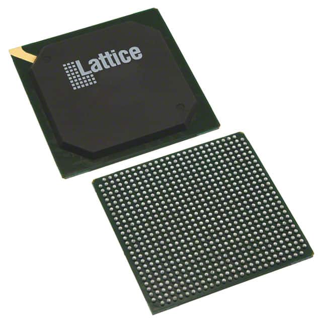
LFE3-35EA-6LFN672I
Product Overview
Category
The LFE3-35EA-6LFN672I belongs to the category of Field Programmable Gate Arrays (FPGAs).
Use
FPGAs are integrated circuits that can be programmed and reprogrammed to perform various digital functions. The LFE3-35EA-6LFN672I is specifically designed for applications requiring high-performance and low-power consumption.
Characteristics
- High performance: The LFE3-35EA-6LFN672I offers a combination of high-speed processing and low-latency operation, making it suitable for demanding applications.
- Low power consumption: This FPGA is designed to minimize power usage, making it energy-efficient and suitable for battery-powered devices.
- Versatility: The LFE3-35EA-6LFN672I supports a wide range of digital functions and can be customized to meet specific application requirements.
Package
The LFE3-35EA-6LFN672I comes in a compact package, ensuring easy integration into electronic systems. The package is designed to provide protection against environmental factors such as moisture and electrostatic discharge.
Essence
The essence of the LFE3-35EA-6LFN672I lies in its ability to provide flexible and customizable digital functionality, enabling designers to implement complex logic circuits in a single device.
Packaging/Quantity
The LFE3-35EA-6LFN672I is typically packaged individually and is available in various quantities depending on the manufacturer's specifications.
Specifications
- Logic Elements: 35,000
- Flip-Flops: 68,000
- Block RAM: 2,048 Kbits
- DSP Blocks: 126
- Maximum Operating Frequency: 500 MHz
- I/O Pins: 672
- Voltage Range: 1.2V - 3.3V
Detailed Pin Configuration
The LFE3-35EA-6LFN672I has a total of 672 I/O pins, which can be configured for various purposes such as input, output, or bidirectional communication. The pin configuration is detailed in the manufacturer's datasheet.
Functional Features
- High-speed processing: The LFE3-35EA-6LFN672I offers fast data processing capabilities, making it suitable for applications requiring real-time performance.
- Reconfigurability: This FPGA can be reprogrammed multiple times, allowing for design changes and updates without the need for hardware modifications.
- Low power consumption: The LFE3-35EA-6LFN672I is designed to minimize power usage, making it ideal for battery-powered devices or energy-efficient applications.
- Versatile I/O capabilities: With 672 I/O pins, this FPGA provides flexibility in connecting with external devices and peripherals.
Advantages and Disadvantages
Advantages
- High-performance processing capabilities
- Low power consumption
- Versatility in digital function implementation
- Reconfigurable design for easy updates and modifications
Disadvantages
- Complexity in programming and configuration
- Higher cost compared to other digital logic solutions
- Limited availability of alternative models
Working Principles
The LFE3-35EA-6LFN672I operates based on the principles of configurable logic. It consists of an array of programmable logic elements that can be interconnected to implement complex digital functions. These logic elements can be programmed using Hardware Description Languages (HDL) to define the desired functionality. The resulting configuration is stored in non-volatile memory within the FPGA and can be modified as needed.
Detailed Application Field Plans
The LFE3-35EA-6LFN672I finds applications in various fields, including:
- Communications: It can be used in the development of high-speed data communication systems, such as network routers and switches.
- Industrial Automation: The FPGA's high-performance capabilities make it suitable for controlling and monitoring complex industrial processes.
- Aerospace and Defense: Its reconfigurable nature allows for adaptability in mission-critical applications, such as radar systems and avionics.
- Medical Devices: The FPGA can be utilized in medical imaging equipment, patient monitoring systems, and other healthcare devices requiring real-time processing.
Detailed and Complete Alternative Models
While the LFE3-35EA-6LFN672I offers a unique combination of features, there are alternative models available from different manufacturers that cater to similar requirements. Some notable alternatives include:
- Xilinx Virtex UltraScale+: Offers high-performance processing and advanced features for demanding applications.
- Intel Cyclone V: Provides a balance between performance and cost-effectiveness, suitable for a wide range of applications.
- Microchip PolarFire: Focuses on low-power consumption and security features, making it ideal for IoT and edge computing applications.
These alternative models offer varying specifications and features,
技術ソリューションにおける LFE3-35EA-6LFN672I の適用に関連する 10 件の一般的な質問と回答をリストします。
Sure! Here are 10 common questions and answers related to the application of LFE3-35EA-6LFN672I in technical solutions:
Q: What is the LFE3-35EA-6LFN672I? A: The LFE3-35EA-6LFN672I is a specific model of Field-Programmable Gate Array (FPGA) manufactured by Lattice Semiconductor.
Q: What are the key features of the LFE3-35EA-6LFN672I? A: The key features of this FPGA include 35,000 Look-Up Tables (LUTs), 672 pins, low power consumption, and high-speed performance.
Q: In what applications can the LFE3-35EA-6LFN672I be used? A: This FPGA can be used in various applications such as industrial automation, telecommunications, automotive electronics, medical devices, and more.
Q: How does the LFE3-35EA-6LFN672I contribute to industrial automation? A: It enables the implementation of complex control algorithms, data processing, and communication interfaces required in industrial automation systems.
Q: Can the LFE3-35EA-6LFN672I be used for high-speed data processing? A: Yes, this FPGA offers high-speed performance and can handle data processing tasks efficiently.
Q: Does the LFE3-35EA-6LFN672I support communication protocols? A: Yes, it supports various communication protocols such as UART, SPI, I2C, Ethernet, and CAN, making it suitable for applications requiring connectivity.
Q: Can the LFE3-35EA-6LFN672I be used in safety-critical applications? A: Yes, this FPGA is designed to meet safety standards and can be used in safety-critical applications like automotive electronics and medical devices.
Q: What development tools are available for programming the LFE3-35EA-6LFN672I? A: Lattice Semiconductor provides software tools like Lattice Diamond and Lattice Radiant for designing and programming this FPGA.
Q: Can the LFE3-35EA-6LFN672I be reprogrammed after deployment? A: Yes, being a Field-Programmable device, it can be reprogrammed multiple times, allowing flexibility in design iterations or updates.
Q: Where can I find more information about the LFE3-35EA-6LFN672I? A: You can visit the official website of Lattice Semiconductor or refer to the datasheet and technical documentation provided by the manufacturer for detailed information.
Please note that the specific details and answers may vary depending on the context and requirements of the technical solution.