

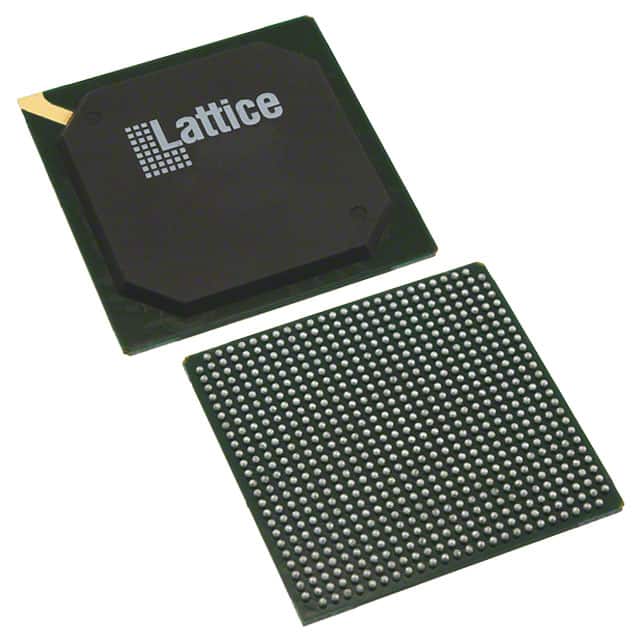
LFE3-35EA-6LFN672C
Product Overview
Category
The LFE3-35EA-6LFN672C belongs to the category of Field Programmable Gate Arrays (FPGAs).
Use
This FPGA is commonly used in various electronic applications for digital logic implementation, prototyping, and system integration.
Characteristics
- High-performance programmable logic device
- Offers flexibility and reconfigurability
- Provides a wide range of logic gates, memory blocks, and I/O interfaces
- Capable of implementing complex digital circuits
- Supports high-speed data processing
Package
The LFE3-35EA-6LFN672C comes in a compact package designed for surface mount technology (SMT). It ensures easy integration onto printed circuit boards (PCBs) and facilitates efficient manufacturing processes.
Essence
The essence of the LFE3-35EA-6LFN672C lies in its ability to provide a customizable and versatile platform for digital circuit design and implementation. It enables engineers to create complex systems with ease and adaptability.
Packaging/Quantity
The LFE3-35EA-6LFN672C is typically packaged in reels or trays, depending on the manufacturer's specifications. The quantity per package varies but is usually sufficient for small to medium-scale production runs.
Specifications
- FPGA Family: LatticeECP3
- Logic Elements: 35,000
- Speed Grade: -6
- Package Type: FCBGA
- Package Pins: 672
- Operating Voltage: 1.2V
- Maximum Frequency: 500 MHz
- Embedded Memory: Up to 4.8 Mb
- I/O Interfaces: LVCMOS, LVDS, SSTL, etc.
- Configuration Method: JTAG, SPI, or Parallel Flash
Detailed Pin Configuration
The LFE3-35EA-6LFN672C has 672 pins, each serving a specific purpose in the FPGA's operation. The pin configuration is detailed in the manufacturer's datasheet and should be consulted for precise information.
Functional Features
1. High-Speed Data Processing
The LFE3-35EA-6LFN672C offers high-speed data processing capabilities, making it suitable for applications that require real-time data handling and rapid computation.
2. Reconfigurability
With its programmable nature, this FPGA allows users to modify and reconfigure the logic design as needed, enabling quick prototyping and system modifications without requiring hardware changes.
3. Versatile I/O Interfaces
The FPGA supports various I/O standards such as LVCMOS, LVDS, and SSTL, providing compatibility with a wide range of external devices and interfaces.
4. Embedded Memory
The LFE3-35EA-6LFN672C incorporates embedded memory blocks, allowing for efficient storage and retrieval of data within the FPGA itself, reducing the need for external memory components.
Advantages and Disadvantages
Advantages
- Flexibility and reconfigurability enable rapid prototyping and system modifications.
- High-performance data processing capabilities facilitate real-time applications.
- Versatile I/O interfaces ensure compatibility with different devices and systems.
- Embedded memory blocks enhance data storage and retrieval efficiency.
Disadvantages
- Steeper learning curve compared to traditional fixed-function integrated circuits.
- Higher power consumption compared to dedicated application-specific integrated circuits (ASICs).
- Limited scalability beyond a certain complexity level.
Working Principles
The LFE3-35EA-6LFN672C operates based on the principles of digital logic design. It consists of configurable logic blocks (CLBs), interconnect resources, and I/O elements. The CLBs can be programmed to implement various logic functions, while the interconnect resources facilitate communication between different blocks. The I/O elements enable interaction with external devices.
Detailed Application Field Plans
The LFE3-35EA-6LFN672C finds applications in a wide range of fields, including but not limited to: - Telecommunications - Industrial automation - Aerospace and defense - Automotive electronics - Medical devices - Consumer electronics
In telecommunications, it can be used for signal processing, protocol implementation, and network infrastructure. In industrial automation, it enables control systems, data acquisition, and monitoring. In aerospace and defense, it supports radar systems, avionics, and secure communications. In automotive electronics, it facilitates advanced driver assistance systems (ADAS) and infotainment. In medical devices, it aids in imaging, diagnostics, and patient monitoring. In consumer electronics, it enables high-performance audio/video processing and gaming.
Detailed and Complete Alternative Models
- Xilinx Virtex UltraScale+ VU9P FPGA
- Intel Stratix 10 GX FPGA
- Microsemi PolarFire FPGA
- QuickLogic EOS S3 FPGA
技術ソリューションにおける LFE3-35EA-6LFN672C の適用に関連する 10 件の一般的な質問と回答をリストします。
Sure! Here are 10 common questions and answers related to the application of LFE3-35EA-6LFN672C in technical solutions:
Q: What is the LFE3-35EA-6LFN672C? A: The LFE3-35EA-6LFN672C is a specific model of Field-Programmable Gate Array (FPGA) manufactured by Lattice Semiconductor.
Q: What are the key features of the LFE3-35EA-6LFN672C? A: The key features of this FPGA include 35,000 Look-Up Tables (LUTs), 672 pins, low power consumption, and high-speed performance.
Q: What are some typical applications for the LFE3-35EA-6LFN672C? A: This FPGA can be used in various applications such as industrial automation, telecommunications, automotive electronics, medical devices, and consumer electronics.
Q: How can I program the LFE3-35EA-6LFN672C? A: The LFE3-35EA-6LFN672C can be programmed using hardware description languages (HDL) like VHDL or Verilog, along with appropriate design tools provided by Lattice Semiconductor.
Q: What is the power supply requirement for the LFE3-35EA-6LFN672C? A: The recommended power supply voltage for this FPGA is typically 1.2V, but it can operate within a range of 1.14V to 1.26V.
Q: Can I use the LFE3-35EA-6LFN672C in a high-temperature environment? A: Yes, this FPGA is designed to operate reliably in a wide temperature range, typically from -40°C to 100°C.
Q: Does the LFE3-35EA-6LFN672C support high-speed serial communication protocols? A: Yes, this FPGA supports various high-speed serial protocols like PCIe, Ethernet, USB, and SATA, making it suitable for applications requiring fast data transfer.
Q: Can I use the LFE3-35EA-6LFN672C for real-time signal processing? A: Absolutely! With its high-performance capabilities, this FPGA is well-suited for real-time signal processing tasks such as image or video processing, audio processing, and digital filtering.
Q: Are there any development boards available for the LFE3-35EA-6LFN672C? A: Yes, Lattice Semiconductor provides development boards specifically designed for this FPGA, which can help in prototyping and testing your technical solutions.
Q: Where can I find more information about the LFE3-35EA-6LFN672C? A: You can visit the official website of Lattice Semiconductor or refer to the datasheet and user manual provided by the manufacturer for detailed information about this FPGA.
Please note that the specific details and answers may vary depending on the manufacturer's documentation and specifications.