

LFE3-150EA-7LFN1156C
Product Overview
Category
The LFE3-150EA-7LFN1156C belongs to the category of Field Programmable Gate Arrays (FPGAs).
Use
This FPGA is commonly used in electronic circuits for various applications, including digital signal processing, telecommunications, and embedded systems.
Characteristics
- High-performance FPGA with advanced features
- Low power consumption
- Large capacity for complex designs
- Flexible and reconfigurable architecture
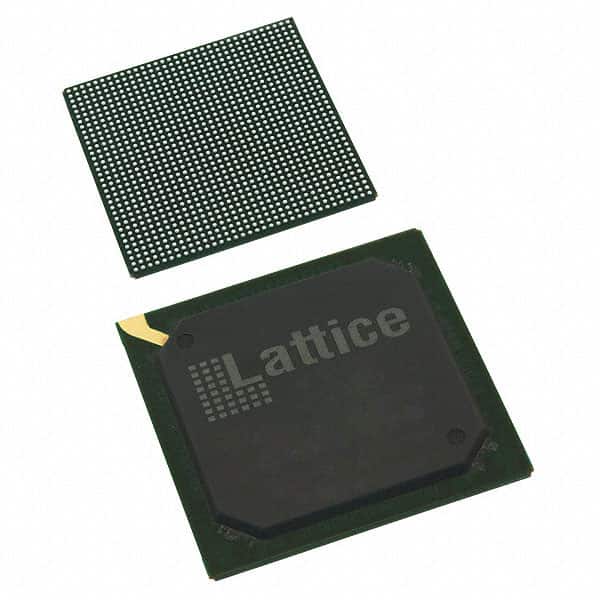
Package
The LFE3-150EA-7LFN1156C comes in a compact package suitable for surface mount technology (SMT) assembly.
Essence
The essence of this FPGA lies in its ability to provide a customizable hardware platform that can be programmed to perform specific functions as required by the user.
Packaging/Quantity
The LFE3-150EA-7LFN1156C is typically packaged in reels or trays, containing a specified quantity of units per package.
Specifications
- FPGA Family: LatticeECP3
- Logic Elements: 149,760
- Embedded Memory: 4,608 Kbits
- Maximum User I/Os: 1,156
- Operating Voltage: 1.2V
- Speed Grade: -7
- Package Type: FCBGA
- Package Pins: 1156
Detailed Pin Configuration
The LFE3-150EA-7LFN1156C has a comprehensive pin configuration, allowing for versatile connectivity and integration within electronic systems. For detailed pin assignments, please refer to the manufacturer's datasheet.
Functional Features
- High-speed performance with low power consumption
- Configurable logic blocks for implementing complex digital circuits
- Dedicated DSP slices for efficient signal processing
- On-chip memory resources for data storage
- Flexible I/O interfaces for seamless integration with external devices
- Clock management resources for precise timing control
Advantages and Disadvantages
Advantages
- High-performance capabilities suitable for demanding applications
- Low power consumption, enabling energy-efficient designs
- Large capacity for accommodating complex designs
- Reconfigurable architecture allows for flexibility in system development
Disadvantages
- Relatively higher cost compared to other programmable logic devices
- Steeper learning curve for beginners due to the complexity of FPGA programming
- Limited availability of alternative models from different manufacturers
Working Principles
The LFE3-150EA-7LFN1156C operates based on the principles of reconfigurable computing. It consists of a matrix of configurable logic blocks interconnected through programmable routing resources. The user can program the FPGA using hardware description languages (HDL) or graphical tools to define the desired functionality. Upon configuration, the FPGA executes the programmed logic, enabling the implementation of various digital circuits.
Detailed Application Field Plans
The LFE3-150EA-7LFN1156C finds extensive application in several fields, including:
- Telecommunications: Used in base stations, routers, and network switches for high-speed data processing and protocol handling.
- Digital Signal Processing: Employed in audio/video processing systems, software-defined radios, and image processing applications.
- Industrial Automation: Utilized in control systems, motor drives, and robotics for real-time control and monitoring.
- Aerospace and Defense: Integrated into radar systems, avionics, and military communication equipment for reliable and secure operations.
- Medical Electronics: Applied in medical imaging devices, patient monitoring systems, and diagnostic equipment for accurate data processing.
Detailed and Complete Alternative Models
While the LFE3-150EA-7LFN1156C is a powerful FPGA, there are alternative models available from different manufacturers that offer similar functionalities. Some notable alternatives include:
- Xilinx Virtex UltraScale+ series
- Intel (formerly Altera) Stratix 10 series
- Microsemi SmartFusion2 series
These alternative models provide a range of options with varying capacities, performance levels, and pricing to suit different project requirements.
In conclusion, the LFE3-150EA-7LFN1156C is a high-performance FPGA that offers flexibility, low power consumption, and large capacity for complex designs. Its application spans various fields, including telecommunications, digital signal processing, and industrial automation. While it has advantages such as its reconfigurable architecture, it also has disadvantages like higher cost and limited availability of alternative models. Understanding its working principles and considering alternative models can help users make informed decisions when incorporating this FPGA into their designs.
技術ソリューションにおける LFE3-150EA-7LFN1156C の適用に関連する 10 件の一般的な質問と回答をリストします。
Sure! Here are 10 common questions and answers related to the application of LFE3-150EA-7LFN1156C in technical solutions:
Q: What is LFE3-150EA-7LFN1156C? A: LFE3-150EA-7LFN1156C is a field-programmable gate array (FPGA) manufactured by Lattice Semiconductor.
Q: What are the key features of LFE3-150EA-7LFN1156C? A: Some key features of LFE3-150EA-7LFN1156C include high logic density, low power consumption, and support for various I/O standards.
Q: In what applications can LFE3-150EA-7LFN1156C be used? A: LFE3-150EA-7LFN1156C can be used in a wide range of applications such as telecommunications, industrial automation, automotive, and aerospace.
Q: How does LFE3-150EA-7LFN1156C help in reducing power consumption? A: LFE3-150EA-7LFN1156C incorporates power-saving features like dynamic power management and clock gating, which help reduce overall power consumption.
Q: Can LFE3-150EA-7LFN1156C support high-speed data transfer? A: Yes, LFE3-150EA-7LFN1156C supports high-speed data transfer through its high-performance I/O interfaces and advanced clocking capabilities.
Q: Is LFE3-150EA-7LFN1156C suitable for real-time signal processing applications? A: Absolutely! LFE3-150EA-7LFN1156C offers high-speed processing capabilities, making it well-suited for real-time signal processing applications.
Q: Can LFE3-150EA-7LFN1156C be reprogrammed after deployment? A: Yes, LFE3-150EA-7LFN1156C is a field-programmable device, meaning it can be reprogrammed even after it has been deployed in a system.
Q: What development tools are available for programming LFE3-150EA-7LFN1156C? A: Lattice Semiconductor provides various development tools like Lattice Diamond and Lattice Radiant, which support the programming of LFE3-150EA-7LFN1156C.
Q: Are there any reference designs or application notes available for LFE3-150EA-7LFN1156C? A: Yes, Lattice Semiconductor provides reference designs and application notes that can help users get started with implementing LFE3-150EA-7LFN1156C in their projects.
Q: Where can I find more information about LFE3-150EA-7LFN1156C? A: You can find more detailed information about LFE3-150EA-7LFN1156C on the official website of Lattice Semiconductor or by referring to the product datasheet and user manual.