

LFE3-150EA-6FN672I
Product Overview
Category
The LFE3-150EA-6FN672I belongs to the category of Field Programmable Gate Arrays (FPGAs).
Use
This FPGA is commonly used in various electronic applications that require high-performance digital logic circuits.
Characteristics
- High-speed and low-power consumption
- Configurable logic blocks
- Flexible interconnectivity
- Large number of input/output pins
- On-chip memory resources
- Support for various communication protocols
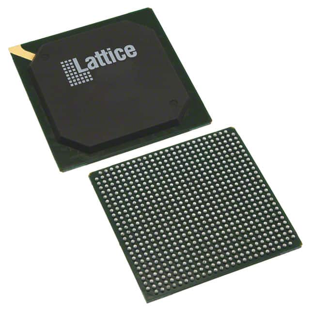
Package
The LFE3-150EA-6FN672I comes in a compact and durable package, ensuring easy integration into electronic systems.
Essence
The essence of this FPGA lies in its ability to be programmed and reconfigured to perform specific tasks, making it highly versatile and adaptable.
Packaging/Quantity
The LFE3-150EA-6FN672I is typically packaged individually and is available in various quantities depending on the manufacturer's specifications.
Specifications
- Model: LFE3-150EA-6FN672I
- Logic Elements: 150,000
- Number of Pins: 672
- Operating Voltage: 1.2V
- Maximum Frequency: 500 MHz
- Embedded Memory: 4.5 Mb
- Configuration Memory: 8 Mb
- Package Type: Fine-pitch Ball Grid Array (FBGA)
Detailed Pin Configuration
The LFE3-150EA-6FN672I has 672 pins, each serving a specific purpose in the overall functionality of the FPGA. The pin configuration includes input/output pins, power supply pins, clock pins, and configuration pins. A detailed pinout diagram can be found in the product datasheet.
Functional Features
- High-speed data processing capabilities
- Configurable logic blocks for custom circuit design
- Flexible interconnectivity for complex system integration
- On-chip memory resources for efficient data storage and retrieval
- Support for various communication protocols, enabling seamless interaction with external devices
Advantages and Disadvantages
Advantages
- Versatile and adaptable to different applications
- High-performance and low-power consumption
- Large number of input/output pins for extensive connectivity options
- Configurable logic blocks allow for custom circuit design
Disadvantages
- Steep learning curve for programming and utilizing the FPGA's full potential
- Higher cost compared to other programmable logic devices
- Limited availability of alternative models with similar specifications
Working Principles
The LFE3-150EA-6FN672I operates based on the principles of reconfigurable digital logic. It consists of configurable logic blocks interconnected through programmable routing resources. The FPGA can be programmed using Hardware Description Languages (HDLs) such as VHDL or Verilog, allowing users to define the desired functionality of the circuit.
Detailed Application Field Plans
The LFE3-150EA-6FN672I finds applications in various fields, including: 1. Telecommunications: Used in network routers and switches for high-speed data processing. 2. Aerospace and Defense: Employed in radar systems, avionics, and military communication equipment. 3. Industrial Automation: Utilized in control systems, robotics, and machine vision applications. 4. Medical Devices: Integrated into medical imaging systems and diagnostic equipment. 5. Automotive: Applied in advanced driver assistance systems (ADAS) and infotainment systems.
Detailed and Complete Alternative Models
While the LFE3-150EA-6FN672I offers a comprehensive set of features, there are alternative FPGA models available in the market that cater to specific requirements. Some notable alternatives include: - Xilinx Virtex UltraScale+ series - Intel Stratix 10 series - Microsemi PolarFire series
These alternative models provide similar capabilities and can be considered based on specific project needs.
In conclusion, the LFE3-150EA-6FN672I is a high-performance FPGA with versatile applications in various industries. Its configurable logic blocks, flexible interconnectivity, and extensive pin configuration make it a powerful tool for designing complex digital circuits. While it may have a learning curve and higher cost, its advantages outweigh the disadvantages, making it a popular choice among engineers and designers.
技術ソリューションにおける LFE3-150EA-6FN672I の適用に関連する 10 件の一般的な質問と回答をリストします。
Question: What is the maximum number of logic elements in LFE3-150EA-6FN672I?
Answer: LFE3-150EA-6FN672I has 149,760 logic elements.Question: What is the operating temperature range for LFE3-150EA-6FN672I?
Answer: The operating temperature range for LFE3-150EA-6FN672I is -40°C to 100°C.Question: Can LFE3-150EA-6FN672I be used for high-speed data processing applications?
Answer: Yes, LFE3-150EA-6FN672I is suitable for high-speed data processing applications.Question: What are the available I/O standards for LFE3-150EA-6FN672I?
Answer: LFE3-150EA-6FN672I supports various I/O standards including LVCMOS, LVTTL, and SSTL.Question: Is LFE3-150EA-6FN672I suitable for power-sensitive designs?
Answer: Yes, LFE3-150EA-6FN672I is designed for low power consumption, making it suitable for power-sensitive designs.Question: Can LFE3-150EA-6FN672I be used in automotive applications?
Answer: Yes, LFE3-150EA-6FN672I is qualified for automotive applications.Question: What are the available package options for LFE3-150EA-6FN672I?
Answer: LFE3-150EA-6FN672I is available in a 672-pin fine-pitch BGA package.Question: Does LFE3-150EA-6FN672I support secure configuration features?
Answer: Yes, LFE3-150EA-6FN672I supports secure configuration features for enhanced system security.Question: Can LFE3-150EA-6FN672I be used in industrial automation applications?
Answer: Yes, LFE3-150EA-6FN672I is suitable for industrial automation applications.Question: What design tools are compatible with LFE3-150EA-6FN672I?
Answer: LFE3-150EA-6FN672I is supported by industry-standard design tools such as Lattice Diamond and iCEcube2.