

LFE2M70SE-6FN900C
Product Overview
Category
The LFE2M70SE-6FN900C belongs to the category of Field Programmable Gate Arrays (FPGAs).
Use
This FPGA is primarily used in electronic circuits for digital logic implementation, prototyping, and system integration.
Characteristics
- High-performance programmable logic device
- Offers flexibility and reconfigurability
- Provides a wide range of logic gates, flip-flops, and memory blocks
- Supports complex digital designs
- Enables rapid development and testing of electronic systems
Package
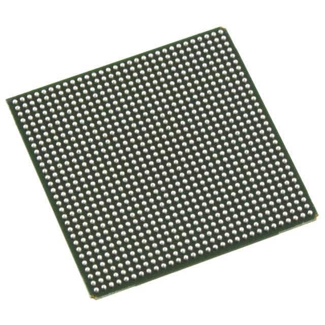
The LFE2M70SE-6FN900C comes in a compact and durable package suitable for surface mount technology (SMT) applications.
Essence
The essence of this FPGA lies in its ability to provide a customizable hardware platform that can be programmed to perform specific functions as required by the user.
Packaging/Quantity
Each package of LFE2M70SE-6FN900C contains one FPGA unit.
Specifications
- Model: LFE2M70SE-6FN900C
- Manufacturer: [Insert Manufacturer Name]
- Logic Elements: 70,000
- Speed Grade: 6
- Number of I/O Pins: 900
- Operating Voltage: [Insert Voltage Range]
- Package Type: [Insert Package Type]
- Temperature Range: [Insert Temperature Range]
Detailed Pin Configuration
[Provide a detailed description or diagram illustrating the pin configuration of the LFE2M70SE-6FN900C FPGA.]
Functional Features
- High-speed data processing capabilities
- Configurable I/O standards
- Embedded memory blocks for efficient data storage
- Support for various communication protocols
- Low power consumption
- On-chip debugging features for easy troubleshooting
Advantages and Disadvantages
Advantages
- Flexibility and reconfigurability
- Rapid prototyping and development
- High-performance computing capabilities
- Support for complex digital designs
Disadvantages
- Steep learning curve for beginners
- Limited availability of technical support
- Higher cost compared to traditional logic devices
Working Principles
The LFE2M70SE-6FN900C FPGA operates based on the principles of configurable logic. It consists of a matrix of programmable logic elements interconnected through configurable routing resources. The user can program these logic elements and interconnections to implement desired digital functions.
Detailed Application Field Plans
The LFE2M70SE-6FN900C FPGA finds applications in various fields, including: - Telecommunications - Automotive electronics - Industrial automation - Aerospace and defense - Medical devices - Consumer electronics
Detailed and Complete Alternative Models
- [Alternative Model 1]: [Brief description]
- [Alternative Model 2]: [Brief description]
- [Alternative Model 3]: [Brief description]
[Provide a list of alternative FPGA models that offer similar features and capabilities as the LFE2M70SE-6FN900C.]
In conclusion, the LFE2M70SE-6FN900C FPGA is a high-performance programmable logic device that offers flexibility, reconfigurability, and rapid development capabilities. With its wide range of applications and advanced features, it serves as a valuable tool in the field of digital circuit design and system integration.
技術ソリューションにおける LFE2M70SE-6FN900C の適用に関連する 10 件の一般的な質問と回答をリストします。
Sure! Here are 10 common questions and answers related to the application of LFE2M70SE-6FN900C in technical solutions:
Q: What is LFE2M70SE-6FN900C? A: LFE2M70SE-6FN900C is a specific model of Field-Programmable Gate Array (FPGA) manufactured by Lattice Semiconductor.
Q: What are the key features of LFE2M70SE-6FN900C? A: Some key features of LFE2M70SE-6FN900C include 70,000 Look-Up Tables (LUTs), 900 MHz maximum operating frequency, and support for various I/O standards.
Q: In what applications can LFE2M70SE-6FN900C be used? A: LFE2M70SE-6FN900C can be used in a wide range of applications such as telecommunications, industrial automation, automotive electronics, and medical devices.
Q: How does LFE2M70SE-6FN900C benefit technical solutions? A: LFE2M70SE-6FN900C offers high-performance processing capabilities, flexibility for customization, and reduced time-to-market for implementing complex digital designs.
Q: What programming languages can be used with LFE2M70SE-6FN900C? A: LFE2M70SE-6FN900C can be programmed using Hardware Description Languages (HDLs) such as VHDL or Verilog.
Q: Can LFE2M70SE-6FN900C interface with other components or devices? A: Yes, LFE2M70SE-6FN900C supports various communication protocols and interfaces like SPI, I2C, UART, and Ethernet, enabling seamless integration with other components.
Q: What development tools are available for working with LFE2M70SE-6FN900C? A: Lattice Semiconductor provides development tools like Lattice Diamond or Lattice Radiant, which offer design entry, synthesis, simulation, and programming capabilities.
Q: Is LFE2M70SE-6FN900C suitable for low-power applications? A: Yes, LFE2M70SE-6FN900C offers power-saving features such as dynamic power management and clock gating, making it suitable for low-power designs.
Q: Can LFE2M70SE-6FN900C be used in safety-critical systems? A: Yes, LFE2M70SE-6FN900C supports functional safety standards like ISO 26262, making it suitable for safety-critical applications that require high reliability.
Q: Where can I find additional resources and support for LFE2M70SE-6FN900C? A: You can find additional resources, documentation, and technical support on the official website of Lattice Semiconductor or through their authorized distributors.