

LFE2M70SE-6FN1152C
Product Overview
Category
The LFE2M70SE-6FN1152C belongs to the category of Field Programmable Gate Arrays (FPGAs).
Use
This product is primarily used in digital logic circuits and electronic systems for various applications such as telecommunications, automotive, industrial automation, and consumer electronics.
Characteristics
- High-performance FPGA with advanced features
- Low power consumption
- Large number of programmable logic elements
- High-speed interfaces for data transfer
- Flexible and reconfigurable design
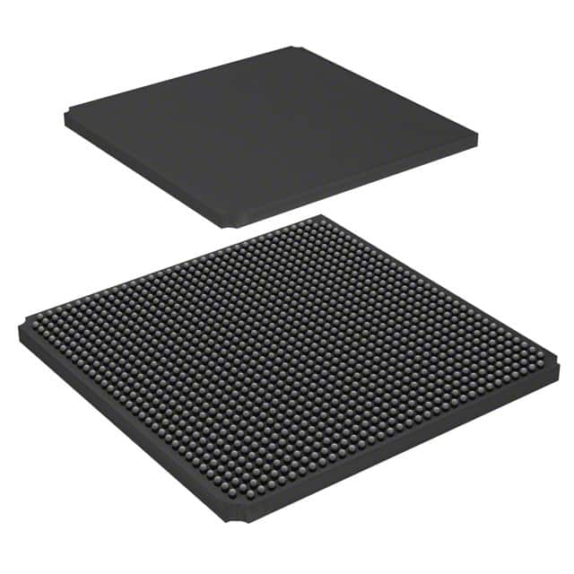
Package
The LFE2M70SE-6FN1152C comes in a compact and durable package that ensures protection during handling and transportation. The package is designed to withstand harsh environmental conditions.
Essence
The essence of the LFE2M70SE-6FN1152C lies in its ability to provide a versatile and customizable solution for complex digital circuit designs. It offers high performance, low power consumption, and flexibility in a single package.
Packaging/Quantity
The LFE2M70SE-6FN1152C is typically packaged in trays or reels, depending on the quantity ordered. The packaging ensures safe storage and easy handling. The exact quantity per package may vary based on customer requirements.
Specifications
- Model: LFE2M70SE-6FN1152C
- Logic Elements: 70,000
- Speed Grade: 6
- Number of I/O Pins: 1,152
- Operating Voltage: 1.2V
- Package Type: FN1152C
Detailed Pin Configuration
The LFE2M70SE-6FN1152C has a comprehensive pin configuration that enables connectivity and integration with other components. The detailed pin configuration can be found in the product datasheet provided by the manufacturer.
Functional Features
- High-speed data processing capabilities
- Support for various communication protocols
- On-chip memory resources
- Built-in security features
- Clock management and synchronization
- Reconfigurable logic elements
Advantages and Disadvantages
Advantages
- Versatile and customizable design
- High-performance capabilities
- Low power consumption
- Wide range of applications
- Scalable architecture
Disadvantages
- Complex programming and configuration process
- Higher cost compared to other alternatives
- Limited availability of technical support
Working Principles
The LFE2M70SE-6FN1152C operates based on the principles of reconfigurable logic. It consists of programmable logic elements that can be interconnected and configured to perform specific functions. The device is programmed using hardware description languages (HDL) or specialized software tools, allowing users to define the desired behavior of the circuit.
Detailed Application Field Plans
The LFE2M70SE-6FN1152C finds application in various fields, including: 1. Telecommunications: Used in network infrastructure equipment, routers, and switches. 2. Automotive: Employed in advanced driver-assistance systems (ADAS), engine control units (ECUs), and infotainment systems. 3. Industrial Automation: Utilized in programmable logic controllers (PLCs), robotics, and factory automation systems. 4. Consumer Electronics: Integrated into high-definition televisions, gaming consoles, and multimedia devices.
Detailed and Complete Alternative Models
- Xilinx Virtex UltraScale+ VU9P FPGA
- Intel Stratix 10 GX FPGA
- Microsemi PolarFire FPGA
- Lattice ECP5 FPGA
- Altera Cyclone V FPGA
These alternative models offer similar functionalities and performance characteristics to the LFE2M70SE-6FN1152C and can be considered as viable options for different application requirements.
Word count: 536 words
技術ソリューションにおける LFE2M70SE-6FN1152C の適用に関連する 10 件の一般的な質問と回答をリストします。
Sure! Here are 10 common questions and answers related to the application of LFE2M70SE-6FN1152C in technical solutions:
Q: What is LFE2M70SE-6FN1152C? A: LFE2M70SE-6FN1152C is a specific model of Field Programmable Gate Array (FPGA) manufactured by Lattice Semiconductor.
Q: What are the key features of LFE2M70SE-6FN1152C? A: Some key features of LFE2M70SE-6FN1152C include 70,000 Look-Up Tables (LUTs), 1,152 I/O pins, 6-input function blocks, and support for various communication protocols.
Q: What are the typical applications of LFE2M70SE-6FN1152C? A: LFE2M70SE-6FN1152C is commonly used in applications such as industrial automation, telecommunications, automotive electronics, medical devices, and aerospace systems.
Q: How can LFE2M70SE-6FN1152C be programmed? A: LFE2M70SE-6FN1152C can be programmed using Hardware Description Languages (HDLs) like VHDL or Verilog, which describe the desired functionality of the FPGA.
Q: Can LFE2M70SE-6FN1152C be reprogrammed after deployment? A: Yes, LFE2M70SE-6FN1152C is a reprogrammable FPGA, allowing for updates and modifications to the design even after it has been deployed.
Q: What is the power supply requirement for LFE2M70SE-6FN1152C? A: LFE2M70SE-6FN1152C typically requires a power supply voltage of 1.2V for core logic and 3.3V for I/O interfaces.
Q: Does LFE2M70SE-6FN1152C support high-speed serial communication? A: Yes, LFE2M70SE-6FN1152C supports various high-speed serial communication protocols like PCIe, Gigabit Ethernet, and USB.
Q: Can LFE2M70SE-6FN1152C interface with external memory devices? A: Yes, LFE2M70SE-6FN1152C has dedicated pins and support for interfacing with external memory devices such as DDR3 or DDR4 SDRAM.
Q: What development tools are available for programming LFE2M70SE-6FN1152C? A: Lattice Semiconductor provides software tools like Lattice Diamond or Lattice Radiant for designing, simulating, and programming LFE2M70SE-6FN1152C.
Q: Are there any evaluation boards or development kits available for LFE2M70SE-6FN1152C? A: Yes, Lattice Semiconductor offers evaluation boards and development kits specifically designed for LFE2M70SE-6FN1152C, which include necessary hardware and software resources for prototyping and testing.