

LFE2M70E-6FN1152C
Product Overview
Category
The LFE2M70E-6FN1152C belongs to the category of Field Programmable Gate Arrays (FPGAs).
Use
FPGAs are integrated circuits that can be programmed and reprogrammed to perform various digital functions. The LFE2M70E-6FN1152C is specifically designed for applications requiring high-performance and low-power consumption.
Characteristics
- High-performance FPGA with low power consumption
- Programmable and reprogrammable
- Suitable for a wide range of applications
- Offers flexibility in design and customization
Package
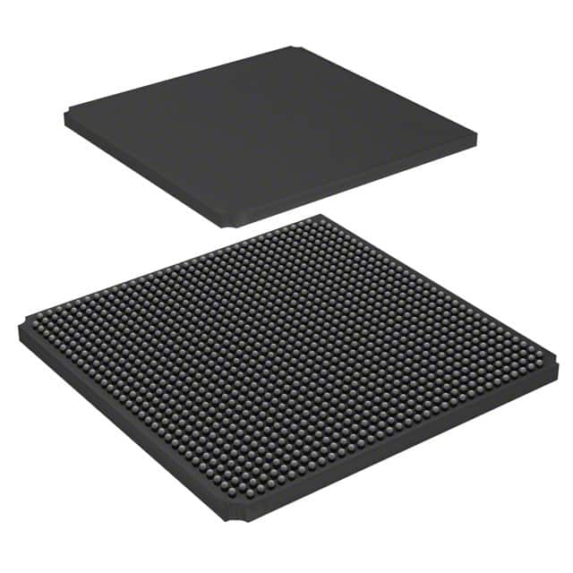
The LFE2M70E-6FN1152C comes in a compact and durable package, ensuring easy handling and protection during transportation and installation.
Essence
The essence of the LFE2M70E-6FN1152C lies in its ability to provide a versatile and efficient solution for digital circuit design and implementation.
Packaging/Quantity
The LFE2M70E-6FN1152C is typically packaged individually and is available in varying quantities depending on the requirements of the user or application.
Specifications
- Model: LFE2M70E-6FN1152C
- Family: Lattice ECP2M
- Logic Elements: 70,000
- Speed Grade: 6
- Number of I/Os: 1,152
- Operating Voltage: 1.2V
- Package Type: FN (FineLine BGA)
- Temperature Range: -40°C to +100°C
Detailed Pin Configuration
The LFE2M70E-6FN1152C has a complex pin configuration with multiple input/output pins, power supply pins, and configuration pins. For a detailed pin configuration diagram, please refer to the product datasheet.
Functional Features
- High-performance FPGA with advanced architecture
- Low power consumption for energy-efficient operation
- Flexible and customizable design options
- Support for various communication protocols and interfaces
- On-chip memory resources for efficient data storage and retrieval
- Built-in security features to protect sensitive information
Advantages and Disadvantages
Advantages
- High-performance capabilities suitable for demanding applications
- Flexibility in design and customization
- Low power consumption for energy efficiency
- Wide range of I/O options for versatile connectivity
- On-chip memory resources for efficient data handling
Disadvantages
- Complex pin configuration may require expertise for proper utilization
- Higher cost compared to other programmable logic devices
- Limited availability of alternative models with similar specifications
Working Principles
The LFE2M70E-6FN1152C operates based on the principles of reconfigurable computing. It consists of a matrix of configurable logic blocks interconnected through programmable routing resources. The device can be programmed using hardware description languages (HDL) or specialized software tools to implement desired digital functions.
Detailed Application Field Plans
The LFE2M70E-6FN1152C finds applications in various fields, including:
- Telecommunications: Used in network infrastructure equipment, such as routers and switches, for high-speed data processing and packet forwarding.
- Industrial Automation: Employed in control systems and robotics for real-time monitoring and control of manufacturing processes.
- Aerospace and Defense: Utilized in radar systems, avionics, and military-grade communication equipment for reliable and secure data processing.
- Medical Devices: Integrated into medical imaging systems, patient monitoring devices, and diagnostic equipment for accurate data analysis and image processing.
- Automotive: Incorporated in advanced driver-assistance systems (ADAS), infotainment systems, and engine control units (ECUs) for enhanced vehicle performance and safety.
Detailed and Complete Alternative Models
While the LFE2M70E-6FN1152C offers unique features and specifications, there are alternative models available in the market that can be considered based on specific requirements. Some notable alternatives include:
- Xilinx Virtex UltraScale+: Offers high-performance capabilities with advanced DSP and memory resources.
- Intel Stratix 10: Provides a combination of high-speed transceivers, low power consumption, and large logic capacity.
- Microsemi PolarFire: Known for its low-power FPGA solutions suitable for applications requiring energy efficiency.
These alternative models offer different trade-offs in terms of performance, power consumption, and cost, allowing users to choose the most suitable option for their specific needs.
Word count: 611 words
技術ソリューションにおける LFE2M70E-6FN1152C の適用に関連する 10 件の一般的な質問と回答をリストします。
Sure! Here are 10 common questions and answers related to the application of LFE2M70E-6FN1152C in technical solutions:
Q: What is the LFE2M70E-6FN1152C? A: The LFE2M70E-6FN1152C is a specific model of Field-Programmable Gate Array (FPGA) manufactured by Lattice Semiconductor.
Q: What are the key features of the LFE2M70E-6FN1152C? A: The key features of this FPGA include 70,000 Look-Up Tables (LUTs), 1,152 I/O pins, low power consumption, and high-speed performance.
Q: What are some typical applications for the LFE2M70E-6FN1152C? A: This FPGA is commonly used in various technical solutions such as telecommunications, industrial automation, automotive electronics, medical devices, and aerospace systems.
Q: How can I program the LFE2M70E-6FN1152C? A: You can program this FPGA using industry-standard hardware description languages (HDLs) like VHDL or Verilog, along with appropriate development tools provided by Lattice Semiconductor.
Q: Can I reprogram the LFE2M70E-6FN1152C after it has been deployed in a system? A: Yes, FPGAs are known for their reprogrammability. You can update the configuration of the LFE2M70E-6FN1152C even after it has been soldered onto a PCB.
Q: What is the power consumption of the LFE2M70E-6FN1152C? A: The power consumption of this FPGA depends on the specific design and utilization. However, it is designed to be power-efficient compared to other similar devices.
Q: Can I interface the LFE2M70E-6FN1152C with other components or microcontrollers? A: Yes, the LFE2M70E-6FN1152C provides a wide range of I/O pins that can be used to interface with other components, microcontrollers, sensors, or communication interfaces.
Q: What is the maximum operating frequency of the LFE2M70E-6FN1152C? A: The maximum operating frequency of this FPGA depends on the specific design and implementation. It can support high-speed applications up to several hundred megahertz or even gigahertz.
Q: Are there any development boards or evaluation kits available for the LFE2M70E-6FN1152C? A: Yes, Lattice Semiconductor offers development boards and evaluation kits specifically designed for the LFE2M70E-6FN1152C, which provide a convenient platform for prototyping and testing.
Q: Where can I find technical documentation and support for the LFE2M70E-6FN1152C? A: You can find technical documentation, datasheets, application notes, and support resources on the official website of Lattice Semiconductor. Additionally, their customer support team can assist you with any specific queries or issues you may have.