

LFE2-70E-5FN672C
Product Overview
Category
The LFE2-70E-5FN672C belongs to the category of Field Programmable Gate Arrays (FPGAs).
Use
This FPGA is designed for various applications in digital logic circuits, including but not limited to telecommunications, automotive, industrial automation, and consumer electronics.
Characteristics
- High-performance FPGA with advanced features
- Low power consumption
- Flexible and reconfigurable design
- High-speed data processing capabilities
- Support for complex algorithms and protocols
Package
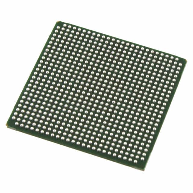
The LFE2-70E-5FN672C comes in a compact and durable package, ensuring easy integration into electronic systems. It is available in a 672-ball FineLine BGA package.
Essence
The essence of the LFE2-70E-5FN672C lies in its ability to provide a customizable and efficient solution for implementing complex digital logic designs.
Packaging/Quantity
The LFE2-70E-5FN672C is typically sold individually or in small quantities, depending on the requirements of the customer or project.
Specifications
- Logic Elements: 70,000
- Embedded Memory: 1,152 Kbits
- Maximum User I/Os: 622
- Block RAM: 4,608 Kbits
- DSP Blocks: 96
- Clock Management Tiles: 8
- Maximum Operating Frequency: 400 MHz
- Voltage Range: 1.14V - 1.26V
Detailed Pin Configuration
The LFE2-70E-5FN672C has a comprehensive pin configuration that allows for versatile connectivity and integration within a system. For detailed pin assignments, please refer to the manufacturer's datasheet.
Functional Features
- High-speed serial transceivers for high-bandwidth data transfer
- Flexible I/O standards for compatibility with various interfaces
- On-chip memory resources for efficient data storage and retrieval
- Dedicated DSP blocks for implementing complex mathematical operations
- Clock management tiles for precise timing control
- Built-in security features to protect sensitive information
Advantages and Disadvantages
Advantages
- High-performance FPGA suitable for demanding applications
- Low power consumption, reducing energy costs
- Reconfigurable design allows for flexibility in system development
- Support for complex algorithms and protocols
- Compact package for easy integration into electronic systems
Disadvantages
- Relatively high cost compared to other programmable logic devices
- Steeper learning curve for inexperienced users
- Limited availability of alternative models with similar specifications
Working Principles
The LFE2-70E-5FN672C operates based on the principles of reconfigurable digital logic. It consists of a large number of configurable logic elements interconnected through programmable routing resources. These logic elements can be programmed to implement desired functionality by configuring their interconnections and behavior.
Detailed Application Field Plans
The LFE2-70E-5FN672C finds applications in various fields, including: 1. Telecommunications: Used in network equipment, base stations, and communication protocols. 2. Automotive: Employed in advanced driver-assistance systems (ADAS), infotainment systems, and engine control units (ECUs). 3. Industrial Automation: Utilized in programmable logic controllers (PLCs), robotics, and process control systems. 4. Consumer Electronics: Integrated into smart TVs, gaming consoles, and home automation systems.
Detailed and Complete Alternative Models
While the LFE2-70E-5FN672C offers a comprehensive set of features, there are alternative models available from different manufacturers that cater to specific requirements. Some notable alternatives include: - Xilinx Virtex UltraScale+ series - Intel Stratix 10 series - Microchip PolarFire series
These alternative models provide similar capabilities and can be considered based on specific project needs.
Word count: 534 words
技術ソリューションにおける LFE2-70E-5FN672C の適用に関連する 10 件の一般的な質問と回答をリストします。
Sure! Here are 10 common questions and answers related to the application of LFE2-70E-5FN672C in technical solutions:
Q: What is the LFE2-70E-5FN672C? A: The LFE2-70E-5FN672C is a field-programmable gate array (FPGA) manufactured by Lattice Semiconductor.
Q: What are the key features of the LFE2-70E-5FN672C? A: The key features of the LFE2-70E-5FN672C include 70,000 lookup tables (LUTs), 672 pins, low power consumption, and high-speed performance.
Q: What are some typical applications for the LFE2-70E-5FN672C? A: The LFE2-70E-5FN672C is commonly used in applications such as telecommunications, industrial automation, automotive electronics, and medical devices.
Q: How can I program the LFE2-70E-5FN672C? A: The LFE2-70E-5FN672C can be programmed using various development tools provided by Lattice Semiconductor, such as the Lattice Diamond software.
Q: What is the power supply voltage range for the LFE2-70E-5FN672C? A: The LFE2-70E-5FN672C operates with a power supply voltage range of 1.14V to 1.26V.
Q: Does the LFE2-70E-5FN672C support different I/O standards? A: Yes, the LFE2-70E-5FN672C supports various I/O standards, including LVCMOS, LVTTL, LVDS, and SSTL.
Q: Can I use the LFE2-70E-5FN672C in a high-temperature environment? A: Yes, the LFE2-70E-5FN672C is designed to operate in a wide temperature range, typically from -40°C to 100°C.
Q: What are the available package options for the LFE2-70E-5FN672C? A: The LFE2-70E-5FN672C is available in a 672-pin FineLine BGA (Ball Grid Array) package.
Q: Does the LFE2-70E-5FN672C have built-in security features? A: Yes, the LFE2-70E-5FN672C provides security features such as bitstream encryption and authentication to protect against unauthorized access.
Q: Where can I find more information about the LFE2-70E-5FN672C? A: You can find more detailed information about the LFE2-70E-5FN672C in the datasheet provided by Lattice Semiconductor or on their official website.