

LCMXO640E-3M100I
Product Overview
Category: Programmable Logic Device (PLD)
Use: The LCMXO640E-3M100I is a high-performance PLD designed for various digital logic applications. It offers flexibility and versatility in implementing complex logic functions.
Characteristics: - Low power consumption - High-speed performance - Small form factor - Easy programmability - Wide operating temperature range
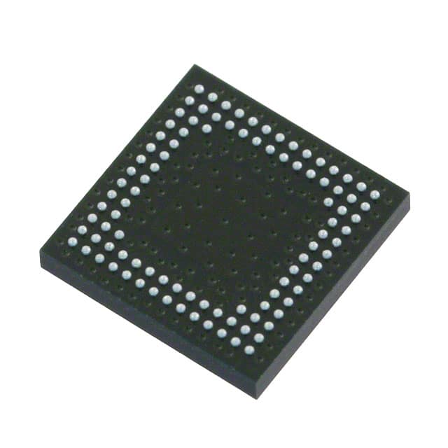
Package: The LCMXO640E-3M100I comes in a 100-pin Quad Flat No-Lead (QFN) package, which provides excellent thermal dissipation and compact size.
Essence: This PLD is built to provide efficient and reliable digital logic implementation in a wide range of applications.
Packaging/Quantity: The LCMXO640E-3M100I is typically sold in reels or trays, with a quantity of 250 units per reel/tray.
Specifications
- Logic Cells: 640
- I/O Pins: 100
- Operating Voltage: 1.2V
- Operating Frequency: Up to 300 MHz
- Programmable Logic Blocks: 40
- Embedded Memory: 64 Kbits
- Maximum User I/Os: 96
- JTAG Boundary Scan Support: Yes
- Package Dimensions: 14mm x 14mm
Detailed Pin Configuration
The LCMXO640E-3M100I has a total of 100 pins, each serving a specific purpose. Here is a brief overview of the pin configuration:
- VCCIO: Power supply voltage for I/O pins
- GND: Ground reference
- VCCINT: Internal power supply voltage
- JTAG: Pins for Joint Test Action Group (JTAG) boundary scan
- I/O Pins: General-purpose input/output pins
- Clock Inputs: Pins for clock signal inputs
- Configuration Pins: Pins for device configuration
For a complete and detailed pin configuration diagram, please refer to the product datasheet.
Functional Features
- High-speed performance allows for efficient execution of complex logic functions.
- Low power consumption ensures energy efficiency in various applications.
- Easy programmability enables quick design iterations and modifications.
- Wide operating temperature range makes it suitable for both commercial and industrial environments.
- JTAG boundary scan support facilitates debugging and testing processes.
Advantages and Disadvantages
Advantages: - High-performance PLD with low power consumption - Compact form factor and wide operating temperature range - Easy programmability for quick design iterations - JTAG boundary scan support for efficient debugging and testing
Disadvantages: - Limited number of logic cells compared to higher-end PLDs - May not be suitable for extremely complex logic designs
Working Principles
The LCMXO640E-3M100I utilizes a combination of configurable logic blocks, embedded memory, and interconnect resources to implement digital logic functions. The device is programmed using hardware description languages (HDL) or schematic entry tools, which define the desired logic behavior. Once programmed, the PLD executes the specified logic operations based on the input signals received.
Detailed Application Field Plans
The LCMXO640E-3M100I finds applications in various fields, including but not limited to: - Industrial automation - Consumer electronics - Automotive systems - Communication equipment - Medical devices
Its versatility and flexibility make it suitable for a wide range of digital logic implementation needs.
Detailed and Complete Alternative Models
- LCMXO256E-3M100I: A lower-capacity version with 256 logic cells and 100 I/O pins.
- LCMXO1200C-4FTN256C: A higher-capacity version with 1200 logic cells and 256 I/O pins.
- LCMXO2-4000HE-5MG132I: A larger PLD with 4000 logic cells and 132 I/O pins.
These alternative models offer different capacity and pin configurations to cater to specific project requirements.
Word count: 446 words
技術ソリューションにおける LCMXO640E-3M100I の適用に関連する 10 件の一般的な質問と回答をリストします。
Sure! Here are 10 common questions and answers related to the application of LCMXO640E-3M100I in technical solutions:
Q: What is the LCMXO640E-3M100I? A: The LCMXO640E-3M100I is a low-cost, low-power FPGA (Field-Programmable Gate Array) device manufactured by Lattice Semiconductor.
Q: What are the key features of the LCMXO640E-3M100I? A: The key features include 640 LUTs (Look-Up Tables), 64 I/O pins, 4 multipliers, 8Kbits of embedded memory, and support for various I/O standards.
Q: What are some typical applications of the LCMXO640E-3M100I? A: The LCMXO640E-3M100I is commonly used in applications such as industrial control systems, consumer electronics, communication devices, and automotive systems.
Q: How can I program the LCMXO640E-3M100I? A: The LCMXO640E-3M100I can be programmed using Lattice Diamond or Lattice Radiant software tools, which provide a graphical interface for designing and programming the FPGA.
Q: Can I reprogram the LCMXO640E-3M100I after it has been programmed once? A: Yes, the LCMXO640E-3M100I is a reprogrammable FPGA, allowing you to modify and update the design as needed.
Q: What voltage levels does the LCMXO640E-3M100I support? A: The LCMXO640E-3M100I supports both 3.3V and 1.2V voltage levels, making it compatible with a wide range of systems.
Q: Can I interface the LCMXO640E-3M100I with other components or microcontrollers? A: Yes, the LCMXO640E-3M100I has multiple I/O pins that can be used to interface with other components or microcontrollers in your system.
Q: What is the power consumption of the LCMXO640E-3M100I? A: The LCMXO640E-3M100I is designed to be low-power, with typical power consumption ranging from a few milliwatts to a few watts, depending on the application.
Q: Does the LCMXO640E-3M100I support any specific communication protocols? A: The LCMXO640E-3M100I supports various communication protocols such as SPI, I2C, UART, and GPIO, allowing for easy integration into different systems.
Q: Where can I find more information about the LCMXO640E-3M100I? A: You can find more detailed information about the LCMXO640E-3M100I, including datasheets, application notes, and reference designs, on the official website of Lattice Semiconductor or by contacting their technical support team.