

LCMXO640E-3M100C
Product Overview
Category
LCMXO640E-3M100C belongs to the category of Field Programmable Gate Arrays (FPGAs).
Use
This product is commonly used in digital logic circuits and electronic systems for various applications.
Characteristics
- LCMXO640E-3M100C is a high-performance FPGA with advanced features.
- It offers a large number of programmable logic cells, allowing for complex designs.
- The device supports various I/O standards, making it versatile for different interfaces.
- It has low power consumption, making it suitable for battery-powered applications.
- LCMXO640E-3M100C provides excellent performance and reliability.
Package and Quantity
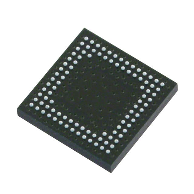
The LCMXO640E-3M100C FPGA is available in a compact 100-pin Quad Flat No-Lead (QFN) package. Each package contains one unit of the FPGA.
Specifications
- Logic Cells: 640
- Maximum Frequency: 100 MHz
- I/O Pins: 100
- Operating Voltage: 3.3V
- Configuration Memory: Flash-based
- Package Type: QFN
- Package Dimensions: 10mm x 10mm
Pin Configuration
The pin configuration of LCMXO640E-3M100C is as follows:
| Pin Number | Pin Name | Description | |------------|----------|-------------| | 1 | VCCIO | I/O Power Supply Voltage | | 2 | GND | Ground | | 3 | IO1 | General Purpose I/O Pin 1 | | ... | ... | ... | | 100 | IO100 | General Purpose I/O Pin 100 |
Functional Features
- LCMXO640E-3M100C offers a wide range of programmable logic cells, allowing for complex digital designs.
- It supports various I/O standards such as LVCMOS, LVTTL, and LVDS, enabling compatibility with different interfaces.
- The FPGA has built-in memory blocks that can be used for data storage or FIFO implementation.
- It provides dedicated clock management resources for precise timing control.
- LCMXO640E-3M100C supports on-chip debugging and configuration through JTAG interface.
Advantages and Disadvantages
Advantages
- High-performance FPGA suitable for complex designs.
- Low power consumption makes it ideal for battery-powered applications.
- Versatile I/O standards support various interface requirements.
- Compact package size allows for space-efficient designs.
- Flash-based configuration memory enables easy reprogramming.
Disadvantages
- Limited number of logic cells compared to higher-end FPGAs.
- Relatively smaller package size may limit the number of I/O pins available for larger designs.
- Higher cost compared to simpler programmable logic devices.
Working Principles
LCMXO640E-3M100C is based on the principle of field-programmable gate arrays. It consists of an array of programmable logic cells interconnected through configurable routing resources. These logic cells can be programmed to implement desired digital logic functions. The configuration of the FPGA is stored in non-volatile memory, allowing for reprogramming as needed.
During operation, the input signals are processed by the programmable logic cells according to the user-defined design. The output signals are then routed through the configurable interconnects to the desired output pins. The FPGA's performance and functionality depend on the complexity of the design and the utilization of its resources.
Application Field Plans
LCMXO640E-3M100C finds applications in various fields, including:
- Communications: Used in wireless communication systems, base stations, and network equipment.
- Industrial Control: Employed in programmable logic controllers (PLCs) and automation systems.
- Consumer Electronics: Integrated into high-performance audio/video processing devices and gaming consoles.
- Medical Devices: Utilized in medical imaging systems and diagnostic equipment.
- Aerospace and Defense: Used in radar systems, avionics, and military communication systems.
Alternative Models
- LCMXO256E-3M100C: A lower-capacity version of the same FPGA family with 256 logic cells.
- LCMXO1200C-3M100C: A higher-capacity FPGA with 1200 logic cells for more complex designs.
- LCMXO640C-3MN132C: An alternative variant with different package type and pin configuration.
These alternative models provide options with varying capacities and features to suit different design requirements.
In conclusion, LCMXO640E-3M100C is a versatile FPGA offering high performance, low power consumption, and compatibility with various I/O standards. Its compact size and flash-based configuration memory make it suitable for a wide range
技術ソリューションにおける LCMXO640E-3M100C の適用に関連する 10 件の一般的な質問と回答をリストします。
Sure! Here are 10 common questions and answers related to the application of LCMXO640E-3M100C in technical solutions:
Question: What is the LCMXO640E-3M100C?
Answer: The LCMXO640E-3M100C is a low-cost, low-power FPGA (Field-Programmable Gate Array) device manufactured by Lattice Semiconductor.Question: What are the key features of the LCMXO640E-3M100C?
Answer: Some key features include 640 LUTs (Look-Up Tables), 64 I/O pins, 4Kbits of embedded memory, and support for various I/O standards.Question: What are some typical applications of the LCMXO640E-3M100C?
Answer: The LCMXO640E-3M100C is commonly used in applications such as industrial control systems, consumer electronics, automotive systems, and communication devices.Question: How can I program the LCMXO640E-3M100C?
Answer: The LCMXO640E-3M100C can be programmed using Lattice's proprietary design software called Diamond Programmer or through third-party tools that support Lattice FPGAs.Question: What voltage levels does the LCMXO640E-3M100C support?
Answer: The LCMXO640E-3M100C supports both 3.3V and 1.2V power supply voltages, making it compatible with a wide range of systems.Question: Can I use the LCMXO640E-3M100C for high-speed applications?
Answer: While the LCMXO640E-3M100C is not specifically designed for high-speed applications, it can still handle moderate data rates and perform various tasks efficiently.Question: Does the LCMXO640E-3M100C have any built-in security features?
Answer: Yes, the LCMXO640E-3M100C provides bitstream encryption and authentication features to protect your design IP from unauthorized access.Question: Can I use the LCMXO640E-3M100C in harsh environments?
Answer: The LCMXO640E-3M100C has a wide operating temperature range and is suitable for use in industrial environments with proper precautions.Question: Are there any development boards available for the LCMXO640E-3M100C?
Answer: Yes, Lattice Semiconductor offers development boards like the iCE40 UltraPlus Breakout Board that can be used with the LCMXO640E-3M100C for prototyping and evaluation.Question: Where can I find more information about the LCMXO640E-3M100C?
Answer: You can find detailed technical documentation, datasheets, and application notes on Lattice Semiconductor's official website or by contacting their support team.