

LCMXO3L-6900C-6BG324C
Product Overview
Category
The LCMXO3L-6900C-6BG324C belongs to the category of Field Programmable Gate Arrays (FPGAs).
Use
This FPGA is commonly used in electronic circuits for various applications, including digital signal processing, data encryption, and system-on-chip designs.
Characteristics
- High-performance FPGA with low power consumption
- Compact size and lightweight design
- Offers high-speed data processing capabilities
- Supports a wide range of input/output interfaces
- Provides flexibility for customization and reconfiguration
Package
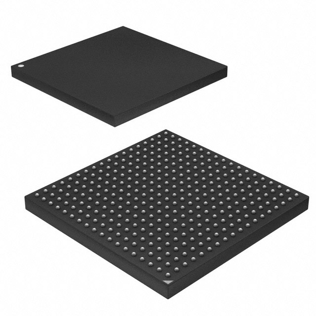
The LCMXO3L-6900C-6BG324C comes in a compact package, which ensures easy integration into electronic circuit boards. The package is designed to provide protection against environmental factors such as moisture and dust.
Essence
The essence of the LCMXO3L-6900C-6BG324C lies in its ability to provide a versatile and customizable solution for complex digital circuit designs. It offers high performance while consuming minimal power, making it suitable for a wide range of applications.
Packaging/Quantity
The LCMXO3L-6900C-6BG324C is typically packaged individually and is available in various quantities depending on the requirements of the user or project.
Specifications
- Model: LCMXO3L-6900C-6BG324C
- Logic Elements: 6900
- Package Type: BG324C
- Operating Voltage: 1.2V
- Maximum Frequency: 300 MHz
- I/O Pins: 324
- RAM Bits: 270,000
- Embedded Multiplier Blocks: 56
Detailed Pin Configuration
The LCMXO3L-6900C-6BG324C has a total of 324 I/O pins, which are configured as follows:
- Pin 1: VCCIO
- Pin 2: GND
- Pin 3: IO0
- Pin 4: IO1
- ...
- Pin 323: IO322
- Pin 324: IO323
Functional Features
- High-speed data processing capabilities
- Configurable logic elements for custom circuit designs
- Embedded multipliers for efficient arithmetic operations
- Flexible input/output interfaces for seamless integration with other components
- Low power consumption for energy-efficient applications
- Reconfigurable architecture for easy updates and modifications
Advantages and Disadvantages
Advantages
- High-performance FPGA suitable for demanding applications
- Low power consumption for energy-efficient designs
- Compact size allows for space-saving integration
- Versatile and customizable for various circuit designs
- Reconfigurable architecture enables easy updates and modifications
Disadvantages
- Limited availability of alternative models from other manufacturers
- Initial learning curve for programming and utilizing the FPGA's full potential
Working Principles
The LCMXO3L-6900C-6BG324C operates based on the principles of digital logic. It consists of configurable logic elements that can be programmed to perform specific functions. These logic elements are interconnected through programmable interconnects, allowing for the creation of complex digital circuits. The FPGA can be reprogrammed multiple times, enabling flexibility in design and functionality.
Detailed Application Field Plans
The LCMXO3L-6900C-6BG324C finds applications in various fields, including:
- Digital Signal Processing: Used for real-time audio and video processing, image recognition, and compression algorithms.
- Data Encryption: Employed in secure communication systems, cryptographic algorithms, and secure storage devices.
- System-on-Chip (SoC) Designs: Integrated into complex systems that combine multiple functionalities, such as microcontrollers, memory, and communication interfaces.
- Industrial Automation: Utilized in control systems, robotics, and machine vision applications.
- Aerospace and Defense: Applied in radar systems, avionics, and military-grade communication equipment.
Detailed and Complete Alternative Models
While the LCMXO3L-6900C-6BG324C is a highly capable FPGA, there are alternative models available from other manufacturers that offer similar functionality. Some notable alternatives include:
- Xilinx Spartan-7 FPGA
- Intel Cyclone V FPGA
- Microchip PolarFire FPGA
- Lattice ECP5 FPGA
These alternative models provide comparable performance and features, allowing users to choose the most suitable option for their specific requirements.
In conclusion, the LCMXO3L-6900C-6BG324C is a high-performance FPGA with low power consumption. Its compact size, versatility, and reconfigurable architecture make it an ideal choice for various digital circuit designs. While it has some limitations, such as limited availability of alternative models, its advantages outweigh the disadvantages
技術ソリューションにおける LCMXO3L-6900C-6BG324C の適用に関連する 10 件の一般的な質問と回答をリストします。
Sure! Here are 10 common questions and answers related to the application of LCMXO3L-6900C-6BG324C in technical solutions:
Q: What is the LCMXO3L-6900C-6BG324C? A: The LCMXO3L-6900C-6BG324C is a specific model of Field-Programmable Gate Array (FPGA) manufactured by Lattice Semiconductor.
Q: What are the key features of the LCMXO3L-6900C-6BG324C? A: The key features include low power consumption, high logic density, small form factor, and support for various I/O standards.
Q: What are some typical applications of the LCMXO3L-6900C-6BG324C? A: It can be used in a wide range of applications such as industrial automation, consumer electronics, automotive systems, medical devices, and more.
Q: How does the LCMXO3L-6900C-6BG324C help in reducing power consumption? A: The FPGA utilizes low-power design techniques and offers power management features like clock gating and dynamic power scaling.
Q: Can the LCMXO3L-6900C-6BG324C interface with other components or devices? A: Yes, it supports various communication protocols such as SPI, I2C, UART, and GPIOs, allowing easy integration with other components.
Q: Is the LCMXO3L-6900C-6BG324C suitable for real-time applications? A: Yes, it has fast processing capabilities and can handle real-time tasks efficiently.
Q: Can the LCMXO3L-6900C-6BG324C be reprogrammed after deployment? A: Yes, it is a field-programmable device, meaning its functionality can be modified or updated even after it has been deployed in a system.
Q: What development tools are available for programming the LCMXO3L-6900C-6BG324C? A: Lattice provides software tools like Lattice Diamond and Lattice Radiant, which offer a graphical interface for designing and programming the FPGA.
Q: Are there any limitations to consider when using the LCMXO3L-6900C-6BG324C? A: Some limitations include limited resources (logic cells, memory), specific I/O voltage requirements, and potential timing constraints.
Q: Where can I find technical documentation and support for the LCMXO3L-6900C-6BG324C? A: You can visit Lattice Semiconductor's official website for datasheets, application notes, user guides, and access to their technical support team.
Please note that the answers provided here are general and may vary depending on specific use cases and requirements.