

LCMXO256E-5M100C
Product Overview
Category
The LCMXO256E-5M100C belongs to the category of Field-Programmable Gate Arrays (FPGAs).
Use
FPGAs are integrated circuits that can be programmed after manufacturing. The LCMXO256E-5M100C is specifically designed for use in various electronic systems, including telecommunications, automotive, industrial automation, and consumer electronics.
Characteristics
- High-performance FPGA with low power consumption
- Offers a large number of logic elements and programmable interconnects
- Provides flexibility for designing complex digital circuits
- Supports high-speed data processing and real-time applications
Package
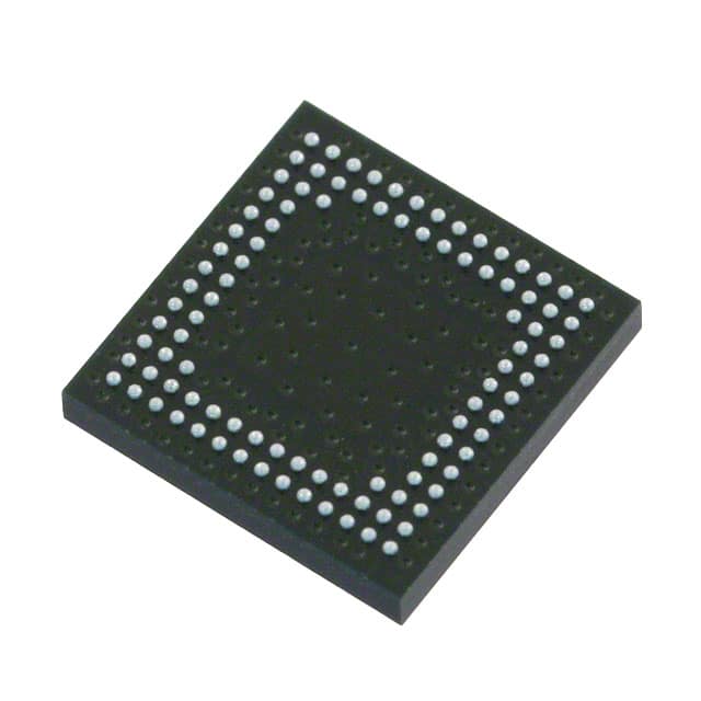
The LCMXO256E-5M100C comes in a compact 100-pin Quad Flat No-Lead (QFN) package. This package type ensures easy integration into circuit boards and allows for efficient heat dissipation.
Essence
The essence of the LCMXO256E-5M100C lies in its ability to provide reconfigurable hardware, enabling designers to implement custom logic functions without the need for dedicated application-specific integrated circuits (ASICs).
Packaging/Quantity
The LCMXO256E-5M100C is typically sold in reels or trays, containing a specific quantity of units per package. The exact packaging and quantity may vary depending on the supplier.
Specifications
- Logic Elements: 2560
- Look-Up Tables (LUTs): 1280
- Flip-Flops: 5120
- Block RAM: 64 Kbits
- Maximum Operating Frequency: 100 MHz
- I/O Pins: 100
- Voltage Range: 1.2V - 3.3V
- Power Consumption: < 150 mW
Detailed Pin Configuration
The LCMXO256E-5M100C has a total of 100 pins, each serving a specific purpose. The pin configuration is as follows:
(Pin Number) (Pin Name) - (Function)
1 - VCCIO - Power supply for I/O banks
2 - GND - Ground reference
3 - IO_0 - General-purpose I/O pin
4 - IO_1 - General-purpose I/O pin
...
99 - IO_98 - General-purpose I/O pin
100 - IO_99 - General-purpose I/O pin
Functional Features
- Reconfigurable logic elements allow for flexible circuit design
- Programmable interconnects enable customization of signal routing
- Dedicated high-speed I/O pins facilitate efficient data transfer
- On-chip memory blocks provide storage for intermediate results
- Built-in clock management resources ensure precise timing control
Advantages and Disadvantages
Advantages
- Versatile and adaptable to various applications
- Reduces time-to-market by eliminating the need for custom ASICs
- Lower development costs compared to traditional hardware solutions
- Allows for in-field updates and modifications
Disadvantages
- Higher power consumption compared to dedicated ASICs
- Limited performance compared to specialized hardware
- Steeper learning curve for designers unfamiliar with FPGA programming
Working Principles
The LCMXO256E-5M100C operates based on the principles of reconfigurable computing. It consists of an array of configurable logic elements interconnected through programmable routing resources. These logic elements can be programmed to implement desired digital circuits using Hardware Description Languages (HDLs) such as VHDL or Verilog. Upon programming, the FPGA executes the specified logic functions, enabling the desired system behavior.
Detailed Application Field Plans
The LCMXO256E-5M100C finds extensive application in various fields, including:
- Telecommunications: Used in base stations, routers, and network switches for high-speed data processing and protocol handling.
- Automotive: Employed in advanced driver-assistance systems (ADAS) for real-time image processing, sensor fusion, and control algorithms.
- Industrial Automation: Utilized in programmable logic controllers (PLCs) for process control, motion control, and machine vision applications.
- Consumer Electronics: Integrated into smart TVs, gaming consoles, and multimedia devices to enable advanced features and connectivity.
Detailed and Complete Alternative Models
- LCMXO2-1200ZE-1MG132C
- LCMXO3LF-6900E-5BG256C
- LCMXO4L-640HC-4SG48C
- LCMXO5LF-2100E-6BG256C
- LCMXO6-4000HE-5TG144C
These alternative models offer varying specifications and capabilities, allowing designers to choose the most suitable FPGA for their specific requirements.
In conclusion, the LCMXO256E-5M100C is
技術ソリューションにおける LCMXO256E-5M100C の適用に関連する 10 件の一般的な質問と回答をリストします。
Sure! Here are 10 common questions and answers related to the application of LCMXO256E-5M100C in technical solutions:
Q: What is the LCMXO256E-5M100C? A: The LCMXO256E-5M100C is a low-cost, low-power FPGA (Field-Programmable Gate Array) device manufactured by Lattice Semiconductor.
Q: What are the key features of the LCMXO256E-5M100C? A: Some key features include 256 LUTs (Look-Up Tables), 4Kbits of embedded memory, 32 I/O pins, and support for various I/O standards.
Q: What are some typical applications of the LCMXO256E-5M100C? A: The LCMXO256E-5M100C is commonly used in applications such as industrial control systems, consumer electronics, communication devices, and IoT (Internet of Things) solutions.
Q: How can I program the LCMXO256E-5M100C? A: The LCMXO256E-5M100C can be programmed using the Lattice Diamond design software or other compatible programming tools provided by Lattice Semiconductor.
Q: What voltage levels does the LCMXO256E-5M100C support? A: The LCMXO256E-5M100C supports both 3.3V and 1.2V voltage levels, making it compatible with a wide range of digital systems.
Q: Can I use the LCMXO256E-5M100C in battery-powered applications? A: Yes, the LCMXO256E-5M100C is designed to be low-power, making it suitable for battery-powered applications where power consumption is a concern.
Q: Can I interface the LCMXO256E-5M100C with other components or microcontrollers? A: Yes, the LCMXO256E-5M100C supports various communication interfaces such as SPI, I2C, UART, and GPIO, allowing easy integration with other components or microcontrollers.
Q: What are the advantages of using an FPGA like the LCMXO256E-5M100C over traditional microcontrollers? A: FPGAs offer greater flexibility and reconfigurability compared to microcontrollers, allowing for custom hardware acceleration, parallel processing, and real-time performance.
Q: Are there any development boards available for the LCMXO256E-5M100C? A: Yes, Lattice Semiconductor provides development boards like the iCEstick Evaluation Kit that can be used for prototyping and testing with the LCMXO256E-5M100C.
Q: Where can I find more resources and support for working with the LCMXO256E-5M100C? A: Lattice Semiconductor's website offers documentation, application notes, reference designs, and a community forum where you can find additional resources and get support for the LCMXO256E-5M100C.