

LCMXO2-4000HE-6MG184I
Product Overview
Category
The LCMXO2-4000HE-6MG184I belongs to the category of Field Programmable Gate Arrays (FPGAs).
Use
FPGAs are integrated circuits that can be programmed and reprogrammed to perform various digital functions. The LCMXO2-4000HE-6MG184I is specifically designed for applications requiring low power consumption and high performance.
Characteristics
- Low power consumption: The LCMXO2-4000HE-6MG184I is optimized for low power operation, making it suitable for battery-powered devices.
- High performance: With a high logic density and fast processing capabilities, this FPGA can handle complex tasks efficiently.
- Small package size: The LCMXO2-4000HE-6MG184I comes in a compact package, making it suitable for space-constrained designs.
- Enhanced security features: This FPGA offers built-in security features to protect sensitive data and intellectual property.
Package and Quantity
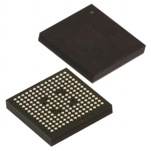
The LCMXO2-4000HE-6MG184I is available in a 184-pin Micro FineLine BGA (Ball Grid Array) package. It is typically sold individually or in small quantities.
Specifications
- Logic Cells: 4000
- Look-Up Tables (LUTs): 4000
- Flip-Flops: 8000
- Block RAM: 112 Kbits
- Maximum Operating Frequency: 150 MHz
- I/O Pins: 184
- Voltage Range: 1.14V - 1.26V
- Operating Temperature Range: -40°C to 85°C
Detailed Pin Configuration
The LCMXO2-4000HE-6MG184I has a total of 184 pins, each serving a specific purpose. The pin configuration includes dedicated input/output pins, power supply pins, and configuration pins. For a detailed pinout diagram and description, please refer to the manufacturer's datasheet.
Functional Features
- Programmable Logic: The LCMXO2-4000HE-6MG184I offers a flexible logic fabric that can be programmed to implement various digital functions.
- I/O Flexibility: With 184 I/O pins, this FPGA provides ample connectivity options for interfacing with external devices.
- Embedded Memory: The built-in block RAM allows for efficient storage and retrieval of data during operation.
- Clock Management: The device supports advanced clocking features such as PLLs (Phase-Locked Loops) for precise timing control.
- Configuration Options: The FPGA can be configured using various methods, including JTAG, SPI, or from an external memory device.
Advantages and Disadvantages
Advantages
- Low power consumption makes it suitable for battery-powered applications.
- High logic density enables complex designs.
- Small package size saves board space.
- Enhanced security features protect sensitive data.
Disadvantages
- Limited number of logic cells compared to higher-end FPGAs.
- May require additional components for certain applications.
- Higher cost compared to other programmable logic devices.
Working Principles
The LCMXO2-4000HE-6MG184I operates based on the principles of reconfigurable computing. It consists of a matrix of configurable logic blocks interconnected through programmable routing resources. The user programs the FPGA by specifying the desired logic functions and interconnections using a hardware description language (HDL). Once programmed, the FPGA executes the specified functions by routing signals through the configured logic blocks.
Detailed Application Field Plans
The LCMXO2-4000HE-6MG184I finds applications in various fields, including:
- Embedded Systems: It can be used to implement control and communication functions in embedded systems such as industrial automation, robotics, and IoT devices.
- Communications: The FPGA can be utilized for signal processing, protocol conversion, and encryption/decryption tasks in communication systems.
- Test and Measurement: It can be employed in test equipment for signal generation, data acquisition, and protocol analysis.
- Consumer Electronics: The FPGA can enhance the functionality and performance of consumer electronic devices like gaming consoles, multimedia players, and smart appliances.
Detailed and Complete Alternative Models
- LCMXO2-1200ZE-1TG144C
- LCMXO2-2000HC-4BG256C
- LCMXO2-4000HC-5MG132C
- LCMXO2-7000HE-6TG144C
These alternative models offer different logic capacities, package options, and performance characteristics. The choice of an alternative model depends on specific project requirements and constraints.
In conclusion, the LCMXO2-4000HE-6MG184I is a low-power, high-performance FPGA that
技術ソリューションにおける LCMXO2-4000HE-6MG184I の適用に関連する 10 件の一般的な質問と回答をリストします。
Sure! Here are 10 common questions and answers related to the application of LCMXO2-4000HE-6MG184I in technical solutions:
Q: What is the LCMXO2-4000HE-6MG184I? A: The LCMXO2-4000HE-6MG184I is a low-cost, low-power FPGA (Field-Programmable Gate Array) device manufactured by Lattice Semiconductor.
Q: What are the key features of the LCMXO2-4000HE-6MG184I? A: Some key features include 4000 Look-Up Tables (LUTs), 128 Kbits of embedded Block RAM, 34 I/O pins, and support for various I/O standards.
Q: What are some typical applications of the LCMXO2-4000HE-6MG184I? A: The LCMXO2-4000HE-6MG184I is commonly used in applications such as industrial control systems, consumer electronics, medical devices, and communication equipment.
Q: How can I program the LCMXO2-4000HE-6MG184I? A: The LCMXO2-4000HE-6MG184I can be programmed using Lattice Diamond or Lattice Radiant software tools, which provide a graphical interface for designing and programming the FPGA.
Q: What voltage levels does the LCMXO2-4000HE-6MG184I support? A: The LCMXO2-4000HE-6MG184I supports both 3.3V and 1.2V voltage levels, making it compatible with a wide range of digital logic circuits.
Q: Can I use the LCMXO2-4000HE-6MG184I in battery-powered applications? A: Yes, the LCMXO2-4000HE-6MG184I is designed to be low-power and can be used in battery-powered applications where power efficiency is crucial.
Q: Does the LCMXO2-4000HE-6MG184I support any communication protocols? A: Yes, the LCMXO2-4000HE-6MG184I supports various communication protocols such as SPI (Serial Peripheral Interface) and I2C (Inter-Integrated Circuit).
Q: Can I interface the LCMXO2-4000HE-6MG184I with other microcontrollers or processors? A: Yes, the LCMXO2-4000HE-6MG184I can be easily interfaced with other microcontrollers or processors using standard communication interfaces like UART or I2C.
Q: Is the LCMXO2-4000HE-6MG184I suitable for high-speed applications? A: While the LCMXO2-4000HE-6MG184I is not specifically designed for high-speed applications, it can still handle moderate-speed digital logic circuits effectively.
Q: Where can I find more information about the LCMXO2-4000HE-6MG184I? A: You can find more detailed information about the LCMXO2-4000HE-6MG184I, including datasheets, application notes, and reference designs, on the official website of Lattice Semiconductor.