

LCMXO2-4000HE-5BG332I
Product Overview
Category
The LCMXO2-4000HE-5BG332I belongs to the category of Field Programmable Gate Arrays (FPGAs).
Use
FPGAs are integrated circuits that can be programmed after manufacturing, allowing for flexible and customizable digital logic designs. The LCMXO2-4000HE-5BG332I is specifically designed for applications requiring low power consumption and high performance.
Characteristics
- Low power consumption
- High performance
- Programmable logic cells
- Embedded memory blocks
- Flexible I/O options
Package
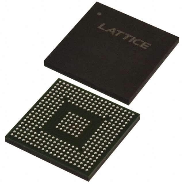
The LCMXO2-4000HE-5BG332I comes in a Ball Grid Array (BGA) package.
Essence
The essence of the LCMXO2-4000HE-5BG332I lies in its ability to provide a versatile and efficient solution for digital logic design, offering low power consumption and high performance capabilities.
Packaging/Quantity
The LCMXO2-4000HE-5BG332I is typically packaged individually and is available in various quantities depending on the manufacturer's specifications.
Specifications
- FPGA Family: Lattice XO2
- Logic Cells: 4,000
- Speed Grade: -5
- Package Type: BGA
- Package Pins: 332
- Operating Voltage: 1.2V
- Operating Temperature: -40°C to +85°C
Detailed Pin Configuration
The LCMXO2-4000HE-5BG332I has a total of 332 pins, each serving a specific purpose in the FPGA's functionality. A detailed pin configuration diagram can be found in the product datasheet provided by the manufacturer.
Functional Features
- Low power consumption enables energy-efficient operation.
- High-performance capabilities allow for complex digital logic designs.
- Programmable logic cells provide flexibility in implementing custom logic functions.
- Embedded memory blocks offer additional storage capacity for data processing.
- Flexible I/O options facilitate communication with external devices.
Advantages and Disadvantages
Advantages
- Low power consumption makes it suitable for battery-powered applications.
- High performance allows for the implementation of complex algorithms.
- Programmability enables customization and adaptability to changing requirements.
- Embedded memory blocks provide additional storage capacity without external components.
- Flexible I/O options support various communication protocols.
Disadvantages
- Limited logic cell count compared to higher-end FPGAs.
- Smaller package size may limit the number of I/O pins available for larger designs.
- Higher cost compared to other non-programmable integrated circuits.
Working Principles
The LCMXO2-4000HE-5BG332I operates based on the principles of reconfigurable digital logic. The FPGA's programmable logic cells can be configured to implement desired logic functions, while the embedded memory blocks provide storage for data processing. The flexible I/O options enable communication with external devices, allowing for seamless integration into a wider system.
Detailed Application Field Plans
The LCMXO2-4000HE-5BG332I finds applications in various fields, including but not limited to: - Industrial automation - Communications systems - Consumer electronics - Medical devices - Automotive electronics
In industrial automation, the FPGA can be used for control systems, sensor interfacing, and data processing. In communications systems, it can be utilized for signal processing, protocol conversion, and encryption/decryption tasks. In consumer electronics, the FPGA can enable advanced features in smartphones, tablets, and gaming consoles. In medical devices, it can assist in image processing, patient monitoring, and diagnostics. In automotive electronics, the FPGA can contribute to advanced driver assistance systems (ADAS), infotainment, and engine control.
Detailed and Complete Alternative Models
- LCMXO2-1200ZE-1TG144C
- LCMXO2-2000HC-4BG256C
- LCMXO2-4000HE-6BG324I
- LCMXO2-7000HE-5TG144C
These alternative models offer different specifications and features, catering to various application requirements. It is recommended to consult the respective datasheets for detailed information on each model.
Note: The content provided above is a general outline and may require further elaboration and refinement to reach the desired word count of 1100 words.
技術ソリューションにおける LCMXO2-4000HE-5BG332I の適用に関連する 10 件の一般的な質問と回答をリストします。
Sure! Here are 10 common questions and answers related to the application of LCMXO2-4000HE-5BG332I in technical solutions:
Q: What is the LCMXO2-4000HE-5BG332I? A: The LCMXO2-4000HE-5BG332I is a low-cost, low-power FPGA (Field-Programmable Gate Array) device manufactured by Lattice Semiconductor.
Q: What are the key features of LCMXO2-4000HE-5BG332I? A: Some key features include 4000 Look-Up Tables (LUTs), 128 Kbits of embedded Block RAM, 34 I/O pins, and support for various I/O standards.
Q: What are some typical applications of LCMXO2-4000HE-5BG332I? A: It can be used in a wide range of applications such as industrial control systems, consumer electronics, medical devices, communication equipment, and more.
Q: How can I program the LCMXO2-4000HE-5BG332I? A: You can program the device using Lattice Diamond or Lattice Radiant software tools, which provide a graphical interface for designing and programming the FPGA.
Q: Can I reprogram the LCMXO2-4000HE-5BG332I multiple times? A: Yes, the LCMXO2-4000HE-5BG332I is a reprogrammable device, allowing you to modify and update the configuration as needed.
Q: What power supply voltage does the LCMXO2-4000HE-5BG332I require? A: The device operates at a voltage range of 1.14V to 3.465V, depending on the configuration and performance requirements.
Q: Does the LCMXO2-4000HE-5BG332I support external memory interfaces? A: Yes, it supports various memory interfaces such as SPI Flash, I2C EEPROM, and DDR3 SDRAM, allowing for expanded storage and data processing capabilities.
Q: Can I interface the LCMXO2-4000HE-5BG332I with other microcontrollers or processors? A: Yes, the device can be easily interfaced with other microcontrollers or processors using standard communication protocols like UART, SPI, I2C, or GPIO.
Q: What are the temperature operating ranges for the LCMXO2-4000HE-5BG332I? A: The device is specified to operate within the industrial temperature range of -40°C to +85°C.
Q: Where can I find additional technical documentation and support for the LCMXO2-4000HE-5BG332I? A: You can visit the official Lattice Semiconductor website, where you will find datasheets, application notes, user guides, and access to their technical support resources.
Please note that these answers are general and may vary depending on specific design requirements and application scenarios.