

LCMXO2-4000HC-5BG332I
Product Overview
Category: Programmable Logic Device (PLD)
Use: The LCMXO2-4000HC-5BG332I is a high-capacity PLD designed for various digital logic applications. It offers flexibility and customization options, making it suitable for prototyping, testing, and small-scale production.
Characteristics: - High capacity: The LCMXO2-4000HC-5BG332I has a large number of logic elements, allowing for complex designs. - Low power consumption: It operates at low voltage levels, reducing power consumption and heat dissipation. - Fast performance: The device offers high-speed operation, enabling efficient execution of logic functions. - Small form factor: The compact package size makes it suitable for space-constrained applications. - Easy integration: The PLD can be easily integrated into existing systems using standard interfaces.
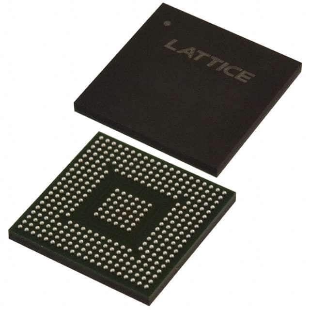
Package: The LCMXO2-4000HC-5BG332I comes in a Ball Grid Array (BGA) package, which provides reliable electrical connections and mechanical stability.
Essence: The essence of the LCMXO2-4000HC-5BG332I lies in its ability to provide programmable logic functionality, allowing users to implement custom digital circuits without the need for dedicated hardware.
Packaging/Quantity: The PLD is typically sold individually or in small quantities, depending on the supplier's packaging options.
Specifications
- Logic Capacity: 4,000 Look-Up Tables (LUTs)
- Number of I/O Pins: 332
- Operating Voltage: 1.2V
- Maximum Frequency: 200 MHz
- Configuration Memory: Flash-based
Pin Configuration
The LCMXO2-4000HC-5BG332I features a total of 332 I/O pins, which are organized into different banks. Each pin serves a specific purpose and can be configured for input or output functionality.
For a detailed pin configuration diagram, please refer to the product datasheet or user manual provided by the manufacturer.
Functional Features
- Programmable Logic: The PLD allows users to define custom logic functions using Look-Up Tables (LUTs) and other configurable elements.
- I/O Flexibility: The device offers a large number of I/O pins, enabling versatile connectivity options with external devices.
- Clock Management: It provides built-in clock management resources, including Phase-Locked Loops (PLLs) for precise timing control.
- Embedded Memory: The PLD includes embedded memory blocks that can be used for data storage or as lookup tables.
- Configuration Options: The device supports various configuration methods, such as JTAG, SPI, or direct programming.
Advantages and Disadvantages
Advantages: - Flexibility: The PLD's programmable nature allows for quick design iterations and customization. - Cost-effective: It eliminates the need for dedicated hardware components, reducing overall system costs. - Time-to-market: The ability to rapidly prototype and test designs accelerates product development cycles. - Power efficiency: The low power consumption of the PLD contributes to energy-efficient operation.
Disadvantages: - Complexity: Programming and configuring the PLD may require specialized knowledge and tools. - Limited capacity: While suitable for many applications, the PLD's capacity may not be sufficient for extremely complex designs. - Non-volatile limitations: The flash-based configuration memory may have limited write endurance compared to other technologies.
Working Principles
The LCMXO2-4000HC-5BG332I operates based on the principles of field-programmable gate arrays (FPGAs). It consists of configurable logic blocks interconnected through programmable routing resources. The PLD's functionality is determined by the configuration data stored in its memory, which can be modified to implement desired logic functions.
Upon power-up or reconfiguration, the PLD loads the configuration data into its internal elements, establishing the desired circuit connections. The device then operates according to the programmed logic, processing input signals and generating output responses based on the defined functionality.
Detailed Application Field Plans
The LCMXO2-4000HC-5BG332I finds applications in various fields, including but not limited to:
- Embedded Systems: The PLD can be used to implement custom interfaces, control systems, or signal processing modules in embedded systems.
- Communications: It enables the development of communication protocols, encryption algorithms, or network interface controllers.
- Industrial Automation: The PLD can be utilized for real-time control, monitoring, or data acquisition in industrial automation systems.
- Test and Measurement: It provides flexible test and measurement capabilities, allowing for the creation of custom testing equipment or data acquisition systems.
- Consumer Electronics: The PLD can be integrated into consumer electronics devices for customized functionality,
技術ソリューションにおける LCMXO2-4000HC-5BG332I の適用に関連する 10 件の一般的な質問と回答をリストします。
Sure! Here are 10 common questions and answers related to the application of LCMXO2-4000HC-5BG332I in technical solutions:
Q: What is the LCMXO2-4000HC-5BG332I? A: The LCMXO2-4000HC-5BG332I is a low-cost, low-power FPGA (Field-Programmable Gate Array) device manufactured by Lattice Semiconductor.
Q: What are the key features of LCMXO2-4000HC-5BG332I? A: Some key features include 4000 Look-Up Tables (LUTs), 332 user I/O pins, low power consumption, and support for various interfaces like SPI, I2C, UART, etc.
Q: What are some typical applications of LCMXO2-4000HC-5BG332I? A: It can be used in a wide range of applications such as industrial automation, consumer electronics, medical devices, communication systems, and IoT (Internet of Things) devices.
Q: How do I program the LCMXO2-4000HC-5BG332I? A: You can program the device using Lattice Diamond or Lattice Radiant software tools, which provide a graphical interface for designing and programming the FPGA.
Q: Can I reprogram the LCMXO2-4000HC-5BG332I multiple times? A: Yes, the LCMXO2-4000HC-5BG332I is a reprogrammable FPGA, allowing you to modify and reconfigure the design multiple times.
Q: What is the power supply requirement for LCMXO2-4000HC-5BG332I? A: The device operates at a voltage range of 1.14V to 3.465V, with typical power consumption varying based on the design and usage.
Q: Can I interface LCMXO2-4000HC-5BG332I with other components or microcontrollers? A: Yes, the FPGA has multiple I/O pins that can be used to interface with other components, microcontrollers, sensors, or communication modules.
Q: Does LCMXO2-4000HC-5BG332I support any specific programming languages? A: The FPGA can be programmed using Hardware Description Languages (HDLs) like VHDL or Verilog, which are commonly used in digital design.
Q: Are there any development boards available for LCMXO2-4000HC-5BG332I? A: Yes, Lattice Semiconductor provides development boards like the LCMXO2-4000HC-5BG332I-ED-EVN, which can be used for prototyping and evaluation.
Q: Where can I find more technical documentation and resources for LCMXO2-4000HC-5BG332I? A: You can visit the official Lattice Semiconductor website or refer to their datasheets, application notes, user guides, and online forums for detailed technical information and support.
Please note that the answers provided here are general and may vary depending on specific requirements and use cases.