

LCMXO1200C-3MN132I
Product Overview
Category
The LCMXO1200C-3MN132I belongs to the category of Field Programmable Gate Arrays (FPGAs).
Use
This product is primarily used in digital logic circuits for various applications such as prototyping, testing, and implementing complex digital systems.
Characteristics
- High flexibility: The LCMXO1200C-3MN132I offers a high degree of flexibility due to its reprogrammable nature, allowing users to modify the functionality of the device even after it has been manufactured.
- Low power consumption: This FPGA is designed to consume minimal power, making it suitable for battery-powered devices or energy-efficient applications.
- High performance: With its advanced architecture and optimized design, the LCMXO1200C-3MN132I delivers high-speed operation and efficient processing capabilities.
- Compact package: The FPGA is packaged in a compact form factor, ensuring easy integration into various electronic systems.
- Abundant resources: It provides a rich set of programmable logic elements, memory blocks, and I/O interfaces, enabling the implementation of complex digital designs.
Packaging/Quantity
The LCMXO1200C-3MN132I is typically available in surface-mount packages. The exact packaging options may vary depending on the manufacturer. It is commonly sold in reels or trays, with quantities ranging from a few units to hundreds or thousands, depending on customer requirements.
Specifications
- Device family: Lattice XO2
- Logic cells: 1200
- Macrocells: 132
- Operating voltage: 1.2V
- Maximum operating frequency: 100 MHz
- I/O standards: LVCMOS, LVTTL, LVDS, SSTL, HSTL, etc.
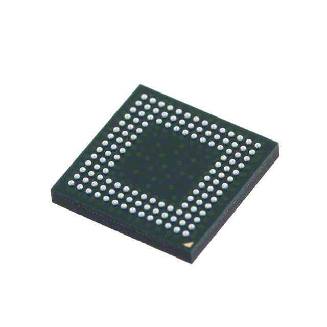
- Package type: QFN
- Package dimensions: 7mm x 7mm
- Temperature range: -40°C to +85°C
Detailed Pin Configuration
The LCMXO1200C-3MN132I has a total of 132 pins, which are assigned for various purposes such as input, output, power supply, and configuration. The pin configuration may vary depending on the specific package variant. Please refer to the manufacturer's datasheet for the detailed pinout information.
Functional Features
- Programmable logic elements: The FPGA offers a large number of configurable logic elements that can be interconnected to implement complex digital functions.
- Memory blocks: It includes dedicated memory blocks that can be used for storing data or implementing lookup tables.
- I/O interfaces: The device provides multiple I/O standards, allowing seamless integration with external devices and systems.
- Clock management: The FPGA features built-in clock management resources, enabling precise control and distribution of clock signals.
- Embedded processors: Some variants of the LCMXO1200C-3MN132I include embedded microprocessors, providing additional processing capabilities.
Advantages and Disadvantages
Advantages
- Flexibility: The reprogrammable nature of FPGAs allows for rapid prototyping and design iterations.
- High performance: FPGAs offer high-speed operation and parallel processing capabilities, making them suitable for demanding applications.
- Low power consumption: Compared to traditional ASICs, FPGAs consume less power, resulting in energy-efficient designs.
- Cost-effective: FPGAs eliminate the need for custom chip fabrication, reducing development costs and time-to-market.
Disadvantages
- Complexity: Designing and programming FPGAs require specialized knowledge and expertise.
- Limited resources: The available logic cells, memory blocks, and I/O pins may impose constraints on the complexity of the design.
- Higher cost per unit: FPGAs tend to have a higher unit cost compared to mass-produced ASICs for large-scale production.
Working Principles
FPGAs are based on a matrix of configurable logic elements interconnected through programmable routing resources. The LCMXO1200C-3MN132I utilizes lookup tables, flip-flops, and other configurable components to implement desired digital functions. The device can be programmed using Hardware Description Languages (HDL) or graphical tools provided by the manufacturer. Once programmed, the FPGA configuration is stored in non-volatile memory and can be reprogrammed as needed.
Detailed Application Field Plans
The LCMXO1200C-3MN132I finds applications in various fields, including but not limited to:
- Communications: Used in wireless base stations, network routers, and data communication equipment.
- Industrial automation: Employed in control systems, robotics, and factory automation.
- Automotive: Integrated into automotive electronics for engine control, infotainment systems, and driver assistance.
- Aerospace and defense: Utilized in avionics, radar systems, and secure communications.
- Medical devices: Incorporated into medical imaging equipment, patient monitoring
技術ソリューションにおける LCMXO1200C-3MN132I の適用に関連する 10 件の一般的な質問と回答をリストします。
Sure! Here are 10 common questions and answers related to the application of LCMXO1200C-3MN132I in technical solutions:
Q: What is the LCMXO1200C-3MN132I? A: The LCMXO1200C-3MN132I is a low-cost, low-power FPGA (Field-Programmable Gate Array) device manufactured by Lattice Semiconductor.
Q: What are the key features of the LCMXO1200C-3MN132I? A: Some key features include 1200 Look-Up Tables (LUTs), 32Kbits of embedded memory, 32 user I/O pins, and support for various I/O standards.
Q: What are some typical applications of the LCMXO1200C-3MN132I? A: The LCMXO1200C-3MN132I is commonly used in applications such as industrial control systems, consumer electronics, communication devices, and automotive systems.
Q: How can I program the LCMXO1200C-3MN132I? A: The LCMXO1200C-3MN132I can be programmed using Lattice Diamond or Lattice Radiant software tools, which provide a graphical interface for designing and programming the FPGA.
Q: What voltage levels does the LCMXO1200C-3MN132I support? A: The LCMXO1200C-3MN132I supports both 3.3V and 1.2V voltage levels, allowing compatibility with a wide range of digital logic circuits.
Q: Can I use the LCMXO1200C-3MN132I in battery-powered applications? A: Yes, the LCMXO1200C-3MN132I is designed to be low-power and can be used in battery-powered applications where power consumption is a concern.
Q: Does the LCMXO1200C-3MN132I support communication interfaces like UART or SPI? A: Yes, the LCMXO1200C-3MN132I supports various communication interfaces, including UART, SPI, I2C, and GPIO, allowing for easy integration with other devices.
Q: Can I reprogram the LCMXO1200C-3MN132I multiple times? A: Yes, the LCMXO1200C-3MN132I is a reprogrammable FPGA, which means you can modify and reprogram it multiple times as per your application requirements.
Q: Are there any development boards available for the LCMXO1200C-3MN132I? A: Yes, Lattice Semiconductor provides development boards specifically designed for the LCMXO1200C-3MN132I, which make it easier to prototype and test your designs.
Q: Where can I find more technical documentation and support for the LCMXO1200C-3MN132I? A: You can find detailed technical documentation, datasheets, application notes, and support resources on the official Lattice Semiconductor website or by contacting their customer support team.
Please note that the answers provided here are general and may vary depending on specific use cases and requirements. It's always recommended to refer to the official documentation and consult with experts for accurate information.