

LC5768MV-75FN484C
Product Overview
Category: Integrated Circuit (IC)
Use: LC5768MV-75FN484C is a high-performance programmable logic device (PLD) designed for various digital applications. It offers flexible and customizable logic functions to meet the specific requirements of different electronic systems.
Characteristics: - High-density integration - Low power consumption - Fast processing speed - Wide operating temperature range - Reliable performance
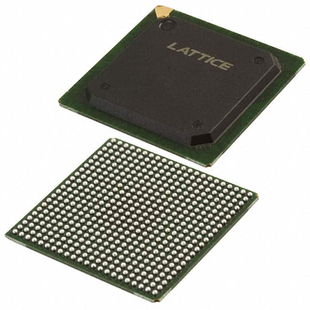
Package: LC5768MV-75FN484C is available in a 484-pin Fine-Pitch Ball Grid Array (FBGA) package, which ensures efficient heat dissipation and compact design.
Essence: LC5768MV-75FN484C is built on advanced semiconductor technology, incorporating a large number of logic gates, flip-flops, and other essential components onto a single chip. This integration allows for complex digital circuitry implementation in a small form factor.
Packaging/Quantity: Each package contains one LC5768MV-75FN484C IC.
Specifications
- Logic Cells: 5,768
- Maximum Operating Frequency: 75 MHz
- Input/Output Pins: 484
- Supply Voltage: 3.3V
- Operating Temperature Range: -40°C to 85°C
- Programmable Logic Blocks: 256
- Embedded Memory: 512 kilobits
- JTAG Boundary Scan Support: Yes
Detailed Pin Configuration
The LC5768MV-75FN484C IC has a total of 484 pins, each serving a specific purpose in the overall functionality of the device. The pin configuration diagram provides detailed information about the assignment and function of each pin.
Functional Features
- Programmability: LC5768MV-75FN484C offers extensive programmability, allowing users to define custom logic functions and implement complex digital designs.
- Flexible I/O Options: The device provides a wide range of input/output options, enabling seamless integration with various external components and systems.
- Embedded Memory: LC5768MV-75FN484C includes embedded memory blocks, which can be utilized for data storage or as lookup tables for implementing specific functions.
- JTAG Boundary Scan: The built-in JTAG boundary scan support facilitates efficient testing and debugging of the device during development and production stages.
Advantages and Disadvantages
Advantages: - High-density integration enables compact system design. - Customizable logic functions cater to diverse application requirements. - Low power consumption contributes to energy-efficient operation. - Fast processing speed enhances overall system performance. - Wide operating temperature range ensures reliability in various environments.
Disadvantages: - Limited availability of alternative models from other manufacturers. - Higher cost compared to lower-end programmable logic devices.
Working Principles
LC5768MV-75FN484C operates based on the principles of digital logic. It consists of numerous interconnected logic gates, flip-flops, and other components that process binary signals (0s and 1s). These components work together to perform logical operations, such as AND, OR, and NOT, allowing the device to execute complex digital functions.
Detailed Application Field Plans
LC5768MV-75FN484C finds applications in various fields, including but not limited to: - Telecommunications - Industrial automation - Consumer electronics - Automotive systems - Medical equipment
In telecommunications, it can be used for signal processing, protocol conversion, and network management. In industrial automation, it enables control and monitoring of machinery and processes. In consumer electronics, it supports multimedia processing and interface connectivity. In automotive systems, it aids in vehicle control and safety features. In medical equipment, it assists in data acquisition and analysis.
Detailed and Complete Alternative Models
While LC5768MV-75FN484C is a highly capable programmable logic device, alternative models from other manufacturers can also be considered. Some notable alternatives include: - Xilinx XC9500XL series - Altera MAX 7000 series - Lattice ispMACH 4000ZE series
These alternative models offer similar functionality and performance characteristics, providing users with options based on their specific requirements.
Word count: 529 words
技術ソリューションにおける LC5768MV-75FN484C の適用に関連する 10 件の一般的な質問と回答をリストします。
Sure! Here are 10 common questions and answers related to the application of LC5768MV-75FN484C in technical solutions:
1. What is LC5768MV-75FN484C? - LC5768MV-75FN484C is a specific model of Field Programmable Gate Array (FPGA) manufactured by Lattice Semiconductor Corporation.
2. What are the key features of LC5768MV-75FN484C? - Some key features of LC5768MV-75FN484C include 5,768 Look-Up Tables (LUTs), 75 MHz maximum operating frequency, 484-pin Fine-Pitch Ball Grid Array (FBGA) package, and support for various I/O standards.
3. What are the typical applications of LC5768MV-75FN484C? - LC5768MV-75FN484C is commonly used in applications such as industrial automation, automotive electronics, telecommunications, medical devices, and consumer electronics.
4. How can LC5768MV-75FN484C be programmed? - LC5768MV-75FN484C can be programmed using Hardware Description Languages (HDLs) like VHDL or Verilog, which describe the desired functionality of the FPGA. The programming can be done using specialized software tools provided by Lattice Semiconductor.
5. Can LC5768MV-75FN484C be reprogrammed after initial programming? - Yes, LC5768MV-75FN484C is a reprogrammable FPGA, allowing for multiple iterations of programming and design changes during the development process.
6. What are the power requirements for LC5768MV-75FN484C? - The power requirements for LC5768MV-75FN484C vary depending on the specific application and usage. It is important to refer to the datasheet and design guidelines provided by Lattice Semiconductor for accurate power supply recommendations.
7. Does LC5768MV-75FN484C support different I/O standards? - Yes, LC5768MV-75FN484C supports various I/O standards such as LVCMOS, LVTTL, LVDS, SSTL, HSTL, and more. The specific I/O standards supported can be found in the device's datasheet.
8. Can LC5768MV-75FN484C interface with other components or devices? - Yes, LC5768MV-75FN484C can interface with other components or devices through its configurable I/O pins. It can communicate with external devices using protocols like SPI, I2C, UART, or custom interfaces implemented in the FPGA design.
9. Are there any development boards or evaluation kits available for LC5768MV-75FN484C? - Yes, Lattice Semiconductor provides development boards and evaluation kits specifically designed for LC5768MV-75FN484C. These kits include necessary hardware and software tools to aid in the development and testing of FPGA designs.
10. Where can I find technical documentation and support for LC5768MV-75FN484C? - Technical documentation, including datasheets, user guides, and application notes, can be found on the official website of Lattice Semiconductor. Additionally, Lattice Semiconductor offers customer support through their online forums, knowledge base, and direct contact channels.