

LC5512MV-75F484C
Product Overview
Category: Integrated Circuit (IC)
Use: The LC5512MV-75F484C is a high-performance programmable logic device designed for various digital applications. It offers versatile functionality and flexibility in designing complex digital systems.
Characteristics: - High-speed operation - Large number of programmable logic elements - Flexible input/output configurations - Low power consumption - Compact package size
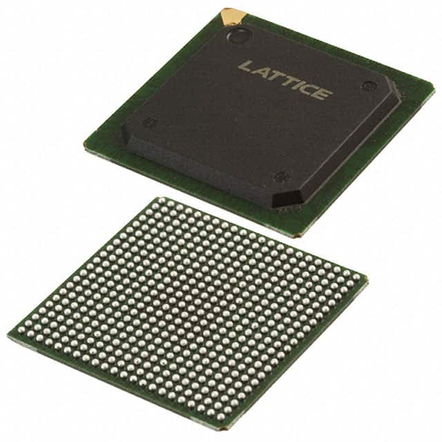
Package: The LC5512MV-75F484C is available in a 484-pin Fine-Pitch Ball Grid Array (FBGA) package, which ensures reliable electrical connections and efficient heat dissipation.
Essence: This IC serves as a key component in digital system design, providing the ability to implement complex logic functions and perform data processing tasks efficiently.
Packaging/Quantity: The LC5512MV-75F484C is typically sold individually in anti-static packaging to prevent damage during transportation and storage.
Specifications
- Logic Capacity: 5120 logic cells
- Number of Inputs/Outputs: 75
- Operating Voltage: 3.3V
- Maximum Frequency: 100 MHz
- Programmable Interconnects: 2560
- On-Chip Memory: 128 Kbits
- Package Dimensions: 23mm x 23mm
Pin Configuration
The LC5512MV-75F484C features a 484-pin FBGA package with pins assigned for various functions. The detailed pin configuration can be found in the product datasheet.
Functional Features
- High-speed operation allows for rapid data processing.
- Large number of programmable logic elements enables complex logic functions to be implemented.
- Flexible input/output configurations provide versatility in connecting with other components.
- Low power consumption ensures energy efficiency.
- On-chip memory facilitates data storage and retrieval.
Advantages and Disadvantages
Advantages: - Versatile functionality for various digital applications. - High-speed operation enables efficient data processing. - Compact package size saves board space. - Low power consumption reduces energy costs.
Disadvantages: - Limited logic capacity compared to some higher-end programmable logic devices. - May require additional support components for certain applications.
Working Principles
The LC5512MV-75F484C operates based on the principles of programmable logic. It consists of a matrix of programmable logic elements interconnected through programmable interconnects. These elements can be configured to perform specific logic functions, allowing the device to implement complex digital systems.
Application Field Plans
The LC5512MV-75F484C finds applications in various fields, including: 1. Telecommunications: Used in network equipment, routers, and switches. 2. Industrial Automation: Employed in control systems and process automation. 3. Consumer Electronics: Integrated into smart home devices, gaming consoles, and multimedia systems. 4. Automotive: Utilized in automotive electronics, such as engine control units and infotainment systems.
Alternative Models
For those seeking alternative options, the following models offer similar functionality: 1. LC5512MV-100F484C: Higher maximum frequency (100 MHz) version of the LC5512MV series. 2. LC5512MV-75F256C: Lower pin count (256-pin) variant with the same logic capacity. 3. LC5512MV-75F400C: Similar pin count (400-pin) option with enhanced I/O capabilities.
These alternative models provide flexibility in choosing the most suitable option based on specific project requirements.
Word Count: 457 words
技術ソリューションにおける LC5512MV-75F484C の適用に関連する 10 件の一般的な質問と回答をリストします。
Sure! Here are 10 common questions and answers related to the application of LC5512MV-75F484C in technical solutions:
Q: What is LC5512MV-75F484C? A: LC5512MV-75F484C is a specific model of Field-Programmable Gate Array (FPGA) manufactured by Lattice Semiconductor.
Q: What are the key features of LC5512MV-75F484C? A: Some key features of LC5512MV-75F484C include 5,512 Look-Up Tables (LUTs), 75 MHz maximum operating frequency, and 484-pin Fine-Pitch Ball Grid Array (FBGA) package.
Q: What are the typical applications of LC5512MV-75F484C? A: LC5512MV-75F484C can be used in various applications such as industrial automation, telecommunications, automotive electronics, medical devices, and consumer electronics.
Q: How can LC5512MV-75F484C be programmed? A: LC5512MV-75F484C can be programmed using Hardware Description Languages (HDLs) like VHDL or Verilog, or through graphical programming tools provided by Lattice Semiconductor.
Q: Can LC5512MV-75F484C interface with other components or devices? A: Yes, LC5512MV-75F484C supports various communication interfaces such as SPI, I2C, UART, and GPIO, allowing it to interface with other components or devices in a system.
Q: What is the power supply requirement for LC5512MV-75F484C? A: LC5512MV-75F484C typically operates at a voltage range of 1.2V to 3.3V, depending on the specific design requirements.
Q: Can LC5512MV-75F484C be reprogrammed after deployment? A: Yes, LC5512MV-75F484C is a reprogrammable FPGA, which means it can be reprogrammed multiple times even after it has been deployed in a system.
Q: Are there any development tools available for designing with LC5512MV-75F484C? A: Yes, Lattice Semiconductor provides development tools like Lattice Diamond and Lattice Radiant, which offer design entry, synthesis, simulation, and programming capabilities for LC5512MV-75F484C.
Q: What are the temperature specifications for LC5512MV-75F484C? A: LC5512MV-75F484C typically operates within a temperature range of -40°C to +100°C, making it suitable for various environments.
Q: Where can I find more information about LC5512MV-75F484C? A: You can find more detailed information about LC5512MV-75F484C, including datasheets, application notes, and reference designs, on the official website of Lattice Semiconductor or by contacting their technical support team.