

LC5512MV-75F256I
Product Overview
Category: Integrated Circuit (IC)
Use: The LC5512MV-75F256I is a high-performance programmable logic device designed for various digital applications. It offers versatile functionality and flexibility in designing complex digital systems.
Characteristics: - High-speed operation - Large capacity - Low power consumption - Programmable logic functions - Flexible pin configuration
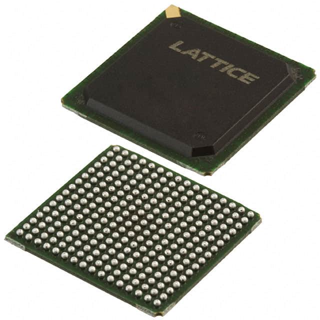
Package: The LC5512MV-75F256I is available in a compact and durable plastic package, ensuring protection against environmental factors and easy integration into electronic circuits.
Essence: This IC serves as a key component in digital system design, providing the ability to implement complex logic functions and perform data processing tasks efficiently.
Packaging/Quantity: The LC5512MV-75F256I is typically packaged in trays or tubes, with each package containing a specified quantity of ICs.
Specifications
- Operating Voltage: 3.3V
- Logic Cells: 5,512
- Maximum Frequency: 75 MHz
- I/O Pins: 256
- Memory Capacity: 256 Kbits
- Package Type: Plastic QFP
Pin Configuration
The LC5512MV-75F256I features a detailed pin configuration, which includes input/output pins, power supply pins, clock pins, and configuration pins. Please refer to the datasheet for the complete pinout diagram.
Functional Features
- Programmable Logic Functions: The LC5512MV-75F256I allows users to program various logic functions, enabling the implementation of custom digital designs.
- High-Speed Operation: With a maximum operating frequency of 75 MHz, this IC ensures fast and efficient data processing.
- Large Capacity: The 256 Kbits memory capacity provides ample space for storing complex logic configurations.
- Low Power Consumption: The IC is designed to minimize power consumption, making it suitable for battery-powered applications.
- Flexible Pin Configuration: The device offers a flexible pin configuration, allowing users to adapt it to their specific application requirements.
Advantages and Disadvantages
Advantages: - Versatile functionality for complex digital designs - High-speed operation for efficient data processing - Large memory capacity for storing complex logic configurations - Low power consumption for energy-efficient applications - Flexible pin configuration for customization
Disadvantages: - Limited availability of alternative models - Relatively high cost compared to simpler logic devices
Working Principles
The LC5512MV-75F256I operates based on the principles of programmable logic. It consists of configurable logic blocks (CLBs), interconnect resources, and input/output blocks (IOBs). The CLBs can be programmed to implement various logic functions, while the interconnect resources provide connections between different CLBs and IOBs. The IOBs handle the input and output signals of the device.
Application Field Plans
The LC5512MV-75F256I finds applications in various fields, including: 1. Telecommunications: Used in network equipment, routers, and switches for data processing and control. 2. Industrial Automation: Employed in programmable logic controllers (PLCs) for process control and automation tasks. 3. Consumer Electronics: Integrated into digital TVs, set-top boxes, and gaming consoles for signal processing and control functions. 4. Automotive: Utilized in automotive electronics for engine control, driver assistance systems, and infotainment systems. 5. Medical Devices: Incorporated into medical equipment for data acquisition, processing, and control.
Alternative Models
While the LC5512MV-75F256I is a highly capable IC, there are alternative models available in the market that offer similar functionality. Some notable alternatives include: - XC95108: A Xilinx CPLD with similar logic capacity and features. - ATF1504: An Atmel FPGA offering comparable performance and flexibility.
These alternative models can be considered based on specific project requirements and availability.
Word count: 511
技術ソリューションにおける LC5512MV-75F256I の適用に関連する 10 件の一般的な質問と回答をリストします。
Sure! Here are 10 common questions and answers related to the application of LC5512MV-75F256I in technical solutions:
Q: What is the LC5512MV-75F256I? A: The LC5512MV-75F256I is a specific model of field-programmable gate array (FPGA) manufactured by Lattice Semiconductor.
Q: What are the key features of the LC5512MV-75F256I? A: Some key features of the LC5512MV-75F256I include 75,000 logic cells, 256 I/O pins, and support for various communication protocols.
Q: What are the typical applications of the LC5512MV-75F256I? A: The LC5512MV-75F256I is commonly used in applications such as industrial automation, telecommunications, automotive systems, and medical devices.
Q: How can I program the LC5512MV-75F256I? A: The LC5512MV-75F256I can be programmed using hardware description languages (HDLs) like VHDL or Verilog, and the programming can be done using software tools provided by Lattice Semiconductor.
Q: Can the LC5512MV-75F256I be reprogrammed after deployment? A: Yes, the LC5512MV-75F256I is a reprogrammable FPGA, which means you can modify its functionality even after it has been deployed in a system.
Q: What are the power requirements for the LC5512MV-75F256I? A: The LC5512MV-75F256I typically operates at a voltage range of 1.14V to 1.26V, and the power consumption depends on the specific design and usage.
Q: Does the LC5512MV-75F256I support high-speed communication interfaces? A: Yes, the LC5512MV-75F256I supports various high-speed communication interfaces like PCIe, Ethernet, USB, and DDR3 memory interfaces.
Q: Can I interface the LC5512MV-75F256I with other microcontrollers or processors? A: Yes, the LC5512MV-75F256I can be easily interfaced with other microcontrollers or processors using standard communication protocols like SPI, I2C, or UART.
Q: Are there any development boards available for the LC5512MV-75F256I? A: Yes, Lattice Semiconductor provides development boards specifically designed for the LC5512MV-75F256I, which include all the necessary components for prototyping and testing.
Q: Where can I find technical documentation and support for the LC5512MV-75F256I? A: You can find technical documentation, datasheets, application notes, and support resources for the LC5512MV-75F256I on the official website of Lattice Semiconductor.