

LC5256MV-75F256C
Product Overview
Category: Integrated Circuit (IC)
Use: The LC5256MV-75F256C is a programmable logic device (PLD) that belongs to the family of Complex Programmable Logic Devices (CPLDs). It is designed for use in various digital applications, including telecommunications, consumer electronics, industrial automation, and automotive systems.
Characteristics: - High-density programmable logic device - Low power consumption - Fast performance - Flexible design options - Easy integration into existing systems
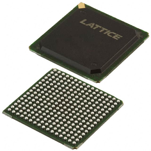
Package: The LC5256MV-75F256C is available in a compact 256-pin Fine-Pitch Ball Grid Array (FBGA) package. This package offers excellent thermal and electrical properties, ensuring reliable operation even in demanding environments.
Essence: The essence of the LC5256MV-75F256C lies in its ability to provide designers with a versatile and efficient solution for implementing complex digital logic functions. Its programmable nature allows for customization and adaptation to specific application requirements.
Packaging/Quantity: The LC5256MV-75F256C is typically sold individually in anti-static packaging to prevent damage during transportation and handling. The exact quantity may vary depending on the supplier or distributor.
Specifications
- Maximum Operating Frequency: 75 MHz
- Number of Macrocells: 256
- Number of I/O Pins: 56
- Supply Voltage: 3.3V
- Operating Temperature Range: -40°C to +85°C
- Programmable Logic Blocks: AND/OR arrays, flip-flops, registers, and interconnect resources
- Programming Method: In-system programmable (ISP) through JTAG interface
Detailed Pin Configuration
The LC5256MV-75F256C features a total of 256 pins, each serving a specific purpose in the device's operation. The pin configuration includes input/output pins, power supply pins, ground pins, and programming interface pins. For a detailed pinout diagram and description, please refer to the manufacturer's datasheet.
Functional Features
- High-speed performance: The LC5256MV-75F256C offers fast operating frequencies, enabling efficient execution of complex digital logic functions.
- Flexible design options: With 256 macrocells and various programmable logic blocks, designers have the flexibility to implement a wide range of digital circuits.
- Low power consumption: The device is designed to minimize power consumption, making it suitable for battery-powered applications.
- In-system programmability: The LC5256MV-75F256C can be programmed in-circuit using the JTAG interface, allowing for easy updates and modifications without the need for physical replacement.
Advantages and Disadvantages
Advantages: - Versatile and flexible design options - High-density integration - Fast performance - Low power consumption - In-system programmability
Disadvantages: - Limited number of I/O pins compared to some other CPLDs - Higher cost compared to simpler programmable logic devices
Working Principles
The LC5256MV-75F256C operates based on the principles of programmable logic. It consists of configurable logic blocks (CLBs) that contain look-up tables (LUTs), flip-flops, and interconnect resources. These CLBs can be interconnected to create complex digital circuits by configuring the LUTs and interconnects through programming.
During operation, the device receives input signals, processes them according to the programmed logic, and produces the desired output signals. The programming of the LC5256MV-75F256C can be done using dedicated software tools provided by the manufacturer.
Detailed Application Field Plans
The LC5256MV-75F256C finds applications in various fields, including:
- Telecommunications: Used in network switches, routers, and communication equipment for signal processing and protocol handling.
- Consumer Electronics: Employed in digital TVs, set-top boxes, and audio/video devices for signal processing, control logic, and user interface implementation.
- Industrial Automation: Utilized in programmable logic controllers (PLCs), motor control systems, and industrial monitoring equipment for process control and automation.
- Automotive Systems: Integrated into automotive electronics for engine management, safety systems, and infotainment applications.
Detailed and Complete Alternative Models
- LC4128V-75T100C: A smaller CPLD with 128 macrocells and 75 MHz maximum operating frequency.
- LC5512MV-75F256I: A higher-density CPLD with 512 macrocells and 75 MHz maximum operating frequency.
- LC4032V-75TN48C: A lower-cost CPLD with 32 macrocells and 75 MHz maximum operating frequency.
These alternative models offer different combinations of density, performance, and cost to cater to specific application requirements.
*Note: The content provided above
技術ソリューションにおける LC5256MV-75F256C の適用に関連する 10 件の一般的な質問と回答をリストします。
Sure! Here are 10 common questions and answers related to the application of LC5256MV-75F256C in technical solutions:
Q: What is LC5256MV-75F256C? A: LC5256MV-75F256C is a specific model of programmable logic device (PLD) manufactured by Lattice Semiconductor.
Q: What are the key features of LC5256MV-75F256C? A: LC5256MV-75F256C offers 256 macrocells, 75MHz maximum operating frequency, and 5V voltage compatibility.
Q: What are some typical applications of LC5256MV-75F256C? A: LC5256MV-75F256C is commonly used in various technical solutions such as industrial control systems, automotive electronics, and telecommunications equipment.
Q: How can LC5256MV-75F256C be programmed? A: LC5256MV-75F256C can be programmed using hardware description languages (HDLs) like VHDL or Verilog, or through proprietary software provided by Lattice Semiconductor.
Q: Can LC5256MV-75F256C be reprogrammed after initial programming? A: No, LC5256MV-75F256C is a one-time programmable (OTP) device and cannot be reprogrammed once it has been programmed.
Q: What is the power supply requirement for LC5256MV-75F256C? A: LC5256MV-75F256C operates on a 5V power supply.
Q: Does LC5256MV-75F256C support external memory interfaces? A: Yes, LC5256MV-75F256C supports various external memory interfaces such as SRAM, SDRAM, and Flash memory.
Q: Can LC5256MV-75F256C interface with other digital components or microcontrollers? A: Yes, LC5256MV-75F256C can interface with other digital components or microcontrollers through standard communication protocols like SPI or I2C.
Q: What is the maximum number of inputs and outputs supported by LC5256MV-75F256C? A: LC5256MV-75F256C supports up to 128 inputs and 64 outputs.
Q: Are there any development tools available for designing with LC5256MV-75F256C? A: Yes, Lattice Semiconductor provides development tools like Lattice Diamond or ispLEVER Classic for designing and programming with LC5256MV-75F256C.
Please note that the answers provided here are general and may vary based on specific requirements and documentation provided by Lattice Semiconductor for LC5256MV-75F256C.