

LC4512V-5T176I
Product Overview
Category
The LC4512V-5T176I belongs to the category of programmable logic devices (PLDs).
Use
This device is primarily used for digital circuit design and implementation. It provides a flexible and customizable solution for various applications.
Characteristics
- Programmable: The LC4512V-5T176I can be programmed to perform specific functions based on the user's requirements.
- High Integration: It offers a high level of integration, allowing multiple logic functions to be implemented within a single device.
- Versatile: This PLD supports a wide range of applications due to its programmability.
- Low Power Consumption: The LC4512V-5T176I is designed to operate efficiently with low power consumption.
Package
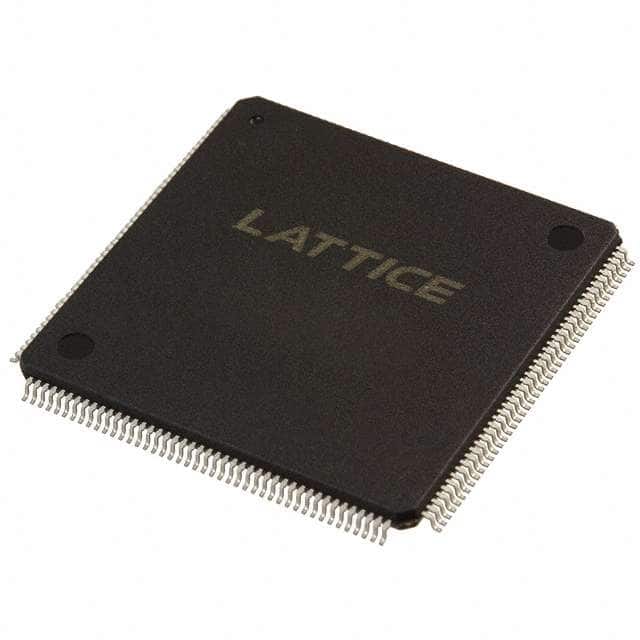
The LC4512V-5T176I comes in a compact package that ensures easy integration into electronic circuits. It is available in a 176-pin Thin Quad Flat Pack (TQFP) package.
Essence
The essence of the LC4512V-5T176I lies in its ability to provide a reconfigurable logic solution, enabling designers to implement complex digital circuits efficiently.
Packaging/Quantity
The LC4512V-5T176I is typically packaged individually and is available in quantities suitable for both prototyping and production purposes.
Specifications
- Logic Cells: 512
- Maximum User I/Os: 176
- Operating Voltage: 3.3V
- Speed Grade: -5
- Programmable Gates: 12,000
- Flip-Flops: 512
- Maximum Frequency: 200 MHz
Detailed Pin Configuration
The LC4512V-5T176I has a total of 176 pins, each serving a specific purpose in the device's operation. The pin configuration is as follows:
(Pin Number) (Pin Name) - (Description)
- VCCIO - Power supply for I/O banks
- GND - Ground reference
- TCK - Test clock input
- TMS - Test mode select
- TDI - Test data input
- TDO - Test data output
- DIN0 - Data input 0
- DIN1 - Data input 1
- DIN2 - Data input 2
- DIN3 - Data input 3 ...
- DOUT175 - Data output 175
Functional Features
- Reconfigurable Logic: The LC4512V-5T176I allows users to modify the logic functions and interconnections within the device, providing flexibility in circuit design.
- In-system Programming: The PLD can be programmed while it is connected to the target system, eliminating the need for separate programming hardware.
- High-Speed Operation: With a maximum operating frequency of 200 MHz, the LC4512V-5T176I can handle complex digital circuits with high-speed requirements.
- I/O Flexibility: The device offers a large number of user I/Os, enabling seamless integration with external components and peripherals.
Advantages and Disadvantages
Advantages
- Flexibility in circuit design due to reconfigurability
- High level of integration reduces component count and board space
- Low power consumption for energy-efficient operation
- In-system programming simplifies the development process
Disadvantages
- Limited resources compared to larger PLDs or FPGAs
- Higher cost per logic cell compared to larger devices
- Steeper learning curve for beginners due to complexity
Working Principles
The LC4512V-5T176I operates based on the principles of programmable logic. It consists of configurable logic blocks (CLBs), interconnect resources, and input/output blocks (IOBs). The CLBs contain look-up tables (LUTs) that can be programmed to implement specific logic functions. The interconnect resources allow for the routing of signals between different CLBs and IOBs. The IOBs provide the interface between the PLD and external components.
Detailed Application Field Plans
The LC4512V-5T176I finds applications in various fields, including:
- Industrial Automation: It can be used to implement control systems, data acquisition modules, and communication interfaces.
- Automotive Electronics: The PLD can be utilized in automotive control units, sensor interfaces, and driver assistance systems.
- Telecommunications: It enables the development of network switches, routers, and protocol converters.
- Consumer Electronics: The device can be employed in smart home devices, gaming consoles, and multimedia systems.
- Medical Devices: It can be integrated into medical imaging equipment, patient monitoring systems, and laboratory instruments.
Detailed and Complete Alternative Models
- LC4032V-5TN48C: A smaller PLD with 32 logic cells and 48 pins, suitable
技術ソリューションにおける LC4512V-5T176I の適用に関連する 10 件の一般的な質問と回答をリストします。
Sure! Here are 10 common questions and answers related to the application of LC4512V-5T176I in technical solutions:
1. What is LC4512V-5T176I? LC4512V-5T176I is a specific model of Field-Programmable Gate Array (FPGA) manufactured by Lattice Semiconductor.
2. What are the key features of LC4512V-5T176I? LC4512V-5T176I offers 512 macrocells, 12 inputs/outputs, 5 ns pin-to-pin delay, and operates at a voltage of 3.3V.
3. What are the typical applications of LC4512V-5T176I? LC4512V-5T176I is commonly used in various technical solutions such as industrial automation, telecommunications, automotive electronics, medical devices, and consumer electronics.
4. How can LC4512V-5T176I be programmed? LC4512V-5T176I can be programmed using Hardware Description Languages (HDLs) like VHDL or Verilog, which describe the desired functionality of the FPGA.
5. Can LC4512V-5T176I be reprogrammed after initial programming? Yes, LC4512V-5T176I is a reprogrammable FPGA, allowing for multiple iterations and updates to the design.
6. What tools are required to program LC4512V-5T176I? To program LC4512V-5T176I, you will need a compatible development board, a programming cable, and software tools provided by Lattice Semiconductor, such as Lattice Diamond or Lattice Radiant.
7. What are the power requirements for LC4512V-5T176I? LC4512V-5T176I operates at a voltage of 3.3V and requires a stable power supply capable of delivering sufficient current to meet the FPGA's power consumption.
8. Can LC4512V-5T176I interface with other components or devices? Yes, LC4512V-5T176I can interface with various components and devices through its input/output pins, allowing for communication with sensors, actuators, memory modules, and other peripherals.
9. Are there any limitations or considerations when using LC4512V-5T176I? Some considerations include the limited number of macrocells and I/O pins, as well as the need for proper signal integrity and timing analysis during the design phase.
10. Where can I find additional resources and support for LC4512V-5T176I? You can find additional resources, documentation, and support for LC4512V-5T176I on the official website of Lattice Semiconductor. They provide datasheets, application notes, reference designs, and a community forum for assistance.