

LC4064B-5TN44I
Product Overview
Category: Integrated Circuit (IC)
Use: The LC4064B-5TN44I is a programmable logic device (PLD) that belongs to the family of Complex Programmable Logic Devices (CPLDs). It is designed for digital circuit applications and offers high-performance, low-power consumption, and flexibility in design.
Characteristics: - High integration level - Low power consumption - Flexible and reprogrammable - Fast propagation delay - Small form factor
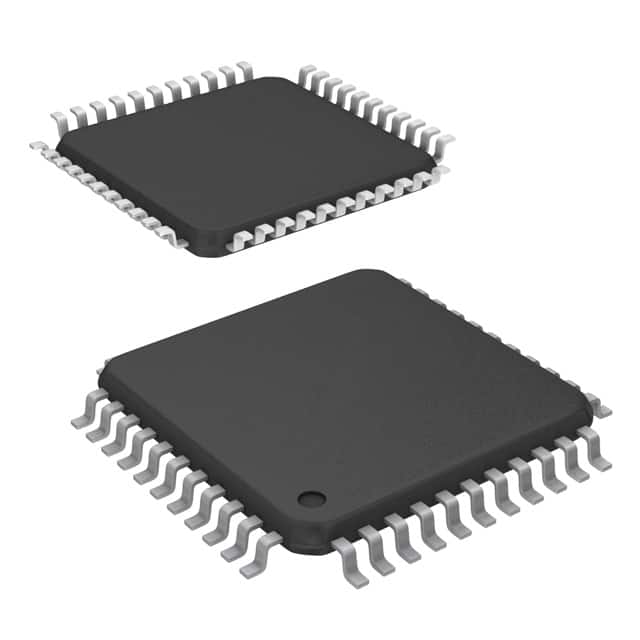
Package: The LC4064B-5TN44I comes in a 44-pin Thin Quad Flat Pack (TQFP) package. This package provides a compact and reliable solution for mounting the IC on a printed circuit board (PCB).
Essence: The essence of the LC4064B-5TN44I lies in its ability to implement complex digital circuits using programmable logic. It allows designers to create custom logic functions by configuring internal resources such as look-up tables, flip-flops, and interconnects.
Packaging/Quantity: The LC4064B-5TN44I is typically sold in reels or tubes containing multiple units. The exact quantity depends on the supplier and customer requirements.
Specifications
- Maximum Gates: 64 macrocells
- Operating Voltage: 3.3V
- Speed Grade: -5
- I/O Pins: 36
- JTAG Boundary Scan Support: Yes
- Operating Temperature Range: -40°C to +85°C
Pin Configuration
The LC4064B-5TN44I has a total of 44 pins. The pinout diagram below illustrates the detailed pin configuration:

Functional Features
- Programmability: The LC4064B-5TN44I can be programmed to implement a wide range of digital logic functions, making it highly versatile for various applications.
- Fast Propagation Delay: The device offers fast signal propagation, enabling efficient operation in time-critical applications.
- Low Power Consumption: The IC is designed to minimize power consumption, making it suitable for battery-powered devices or energy-efficient systems.
- JTAG Boundary Scan Support: The built-in JTAG boundary scan feature allows for easy testing and debugging of the device during development and production stages.
Advantages and Disadvantages
Advantages: - High integration level reduces the need for additional components. - Reprogrammable nature enables design changes without hardware modifications. - Small form factor saves space on PCBs. - Fast propagation delay ensures efficient performance in time-sensitive applications.
Disadvantages: - Limited number of macrocells may restrict the complexity of designs. - Programming and configuration process may require specialized knowledge and tools. - Higher cost compared to simpler logic devices.
Working Principles
The LC4064B-5TN44I utilizes a combination of look-up tables (LUTs), flip-flops, and interconnect resources to implement custom logic functions. The LUTs act as configurable memory elements that store truth tables, while the flip-flops provide sequential logic capabilities. The interconnect resources allow for flexible routing of signals between different logic elements.
During the programming phase, the desired logic functions are defined using a Hardware Description Language (HDL) or a graphical design tool. The configuration data is then loaded into the device, which internally configures the LUTs and interconnects accordingly. Once programmed, the LC4064B-5TN44I operates based on the configured logic functions.
Detailed Application Field Plans
The LC4064B-5TN44I finds applications in various fields, including but not limited to:
- Embedded Systems: The IC can be used in embedded systems for controlling and interfacing with peripheral devices.
- Communications: It can be employed in communication systems for protocol handling, data routing, and signal processing.
- Industrial Automation: The device enables the implementation of control logic in industrial automation systems, such as PLCs (Programmable Logic Controllers).
- Consumer Electronics: It can be utilized in consumer electronic devices for functions like user interface control, data processing, and signal conditioning.
Alternative Models
There are several alternative models available in the market that offer similar functionality to the LC4064B-5TN44I. Some notable alternatives include:
- Xilinx XC9500XL series
- Altera MAX 7000 series
- Lattice ispMACH 4000ZE series
These alternative models provide comparable features and performance, allowing designers to choose the most suitable option based on their specific requirements.
In conclusion, the LC4064B-5TN44I is a versatile programmable logic device that offers high integration, low power consumption, and
技術ソリューションにおける LC4064B-5TN44I の適用に関連する 10 件の一般的な質問と回答をリストします。
Sure! Here are 10 common questions and answers related to the application of LC4064B-5TN44I in technical solutions:
Question: What is LC4064B-5TN44I?
Answer: LC4064B-5TN44I is a specific model of a field-programmable gate array (FPGA) manufactured by Lattice Semiconductor.Question: What are the key features of LC4064B-5TN44I?
Answer: Some key features of LC4064B-5TN44I include 64 macrocells, 64 input/output pins, 4,000 usable gates, and a maximum operating frequency of 133 MHz.Question: In what applications can LC4064B-5TN44I be used?
Answer: LC4064B-5TN44I can be used in various applications such as industrial control systems, automotive electronics, telecommunications, consumer electronics, and more.Question: How can LC4064B-5TN44I be programmed?
Answer: LC4064B-5TN44I can be programmed using hardware description languages (HDLs) like VHDL or Verilog, or through graphical programming tools provided by Lattice Semiconductor.Question: Can LC4064B-5TN44I be reprogrammed after initial programming?
Answer: Yes, LC4064B-5TN44I is a reprogrammable FPGA, which means it can be reprogrammed multiple times to implement different designs or functionalities.Question: What is the power supply requirement for LC4064B-5TN44I?
Answer: LC4064B-5TN44I typically operates on a 3.3V power supply, but it also supports a wide voltage range from 3.0V to 3.6V.Question: Can LC4064B-5TN44I interface with other components or devices?
Answer: Yes, LC4064B-5TN44I can interface with various components and devices through its input/output pins, allowing it to communicate with sensors, actuators, memory modules, and more.Question: What is the maximum operating temperature for LC4064B-5TN44I?
Answer: The maximum operating temperature for LC4064B-5TN44I is typically around 85°C, but it may vary depending on the specific operating conditions.Question: Are there any development tools available for working with LC4064B-5TN44I?
Answer: Yes, Lattice Semiconductor provides development tools like Lattice Diamond or Lattice Radiant software suites that facilitate the design, simulation, and programming of LC4064B-5TN44I.Question: Where can I find more information about LC4064B-5TN44I and its application in technical solutions?
Answer: You can find more detailed information about LC4064B-5TN44I, including datasheets, application notes, and reference designs, on the official website of Lattice Semiconductor or by contacting their technical support team.