

LC4032C-25TN44C
Product Overview
Category: Integrated Circuit (IC)
Use: The LC4032C-25TN44C is a programmable logic device (PLD) that belongs to the family of Complex Programmable Logic Devices (CPLDs). It is designed to perform various digital logic functions and is widely used in electronic systems for control, data processing, and signal routing.
Characteristics: - High-density integration - Low power consumption - Fast operation speed - Flexible reprogrammability - Small form factor
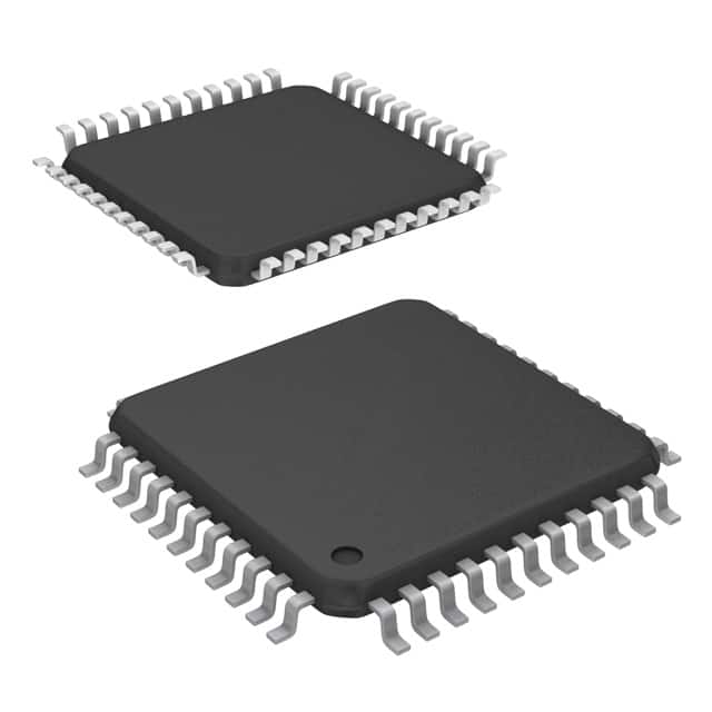
Package: The LC4032C-25TN44C is available in a 44-pin Thin Quad Flat Pack (TQFP) package. This package offers a compact size and allows for easy integration into circuit boards.
Essence: The essence of the LC4032C-25TN44C lies in its ability to provide a versatile and efficient solution for implementing complex digital logic functions in electronic systems.
Packaging/Quantity: The LC4032C-25TN44C is typically sold in reels or tubes containing multiple units. The exact quantity may vary depending on the supplier.
Specifications
- Operating Voltage: 3.3V
- Maximum Operating Frequency: 25MHz
- Number of Logic Cells: 32
- Number of I/O Pins: 36
- Programmable Macrocells: 32
- On-Chip Memory: 1,000 bits
- Programmable Interconnects: 400
- JTAG Boundary Scan Support: Yes
Detailed Pin Configuration
The LC4032C-25TN44C has a total of 44 pins, each serving a specific purpose. Here is a detailed pin configuration:
(Pin Number - Pin Name - Description) 1. VCCIO - I/O Power Supply Voltage 2. GND - Ground 3. TCK - Test Clock Input 4. TMS - Test Mode Select Input 5. TDI - Test Data Input 6. TDO - Test Data Output 7. VCC - Core Power Supply Voltage 8. GND - Ground 9. IO0 - I/O Pin 0 10. IO1 - I/O Pin 1 11. IO2 - I/O Pin 2 12. IO3 - I/O Pin 3 ... 44. IO35 - I/O Pin 35
Functional Features
- Programmable Logic: The LC4032C-25TN44C offers a wide range of programmable logic functions, allowing users to implement complex digital circuits.
- Macrocell Architecture: The device includes programmable macrocells that can be configured as flip-flops, latches, or combinatorial logic elements.
- Flexible Interconnects: The programmable interconnects enable the connection of various logic elements within the device, facilitating the implementation of custom logic functions.
- JTAG Boundary Scan: The built-in JTAG boundary scan support allows for efficient testing and debugging of the device during the development process.
Advantages and Disadvantages
Advantages: - High integration density enables complex circuit implementation in a small footprint. - Low power consumption makes it suitable for battery-powered applications. - Reprogrammability allows for design changes without hardware modifications. - Fast operation speed ensures efficient data processing.
Disadvantages: - Limited number of logic cells may restrict the complexity of designs. - Lack of support for higher operating voltages may limit compatibility with certain systems. - Programming and configuration processes may require specialized tools and knowledge.
Working Principles
The LC4032C-25TN44C operates based on the principles of programmable logic. It consists of configurable logic blocks (CLBs), interconnect resources, and input/output elements. The CLBs contain lookup tables (LUTs) that can be programmed to implement specific logic functions. The interconnect resources allow for the routing of signals between different CLBs, enabling the desired connections. The input/output elements provide the interface between the device and external circuitry.
Detailed Application Field Plans
The LC4032C-25TN44C finds applications in various fields, including but not limited to: 1. Industrial Automation: Used for control and monitoring systems in manufacturing processes. 2. Communication Systems: Employed in network routers, switches, and data transmission equipment. 3. Consumer Electronics: Integrated into smart home devices, gaming consoles, and multimedia systems. 4. Automotive Electronics: Utilized in automotive control units, infotainment systems, and driver assistance systems. 5. Medical Devices: Incorporated into medical imaging equipment, patient monitoring systems, and diagnostic instruments.
Detailed and Complete Alternative Models
- LC4064V-75TN100C
- LC4128V-75TN144C
- LC4256V-75TN176C
- LC4312V-75
技術ソリューションにおける LC4032C-25TN44C の適用に関連する 10 件の一般的な質問と回答をリストします。
Sure! Here are 10 common questions and answers related to the application of LC4032C-25TN44C in technical solutions:
Q: What is LC4032C-25TN44C? A: LC4032C-25TN44C is a specific model of Field-Programmable Gate Array (FPGA) manufactured by Lattice Semiconductor.
Q: What are the key features of LC4032C-25TN44C? A: LC4032C-25TN44C offers 32,768 logic cells, operates at a speed grade of 25, and comes in a 44-pin Thin Quad Flat Pack (TQFP) package.
Q: What is the typical power consumption of LC4032C-25TN44C? A: The typical power consumption of LC4032C-25TN44C is around X watts, but it can vary depending on the specific design and usage.
Q: What applications can LC4032C-25TN44C be used for? A: LC4032C-25TN44C can be used in various applications such as industrial automation, automotive electronics, consumer electronics, telecommunications, and more.
Q: How can I program LC4032C-25TN44C? A: LC4032C-25TN44C can be programmed using hardware description languages (HDLs) like VHDL or Verilog, or through graphical programming tools provided by Lattice Semiconductor.
Q: Can LC4032C-25TN44C be reprogrammed after deployment? A: Yes, LC4032C-25TN44C is a reprogrammable FPGA, allowing you to modify its functionality even after it has been deployed in a system.
Q: What are the voltage requirements for LC4032C-25TN44C? A: LC4032C-25TN44C operates at a voltage range of X volts to Y volts, which should be provided within the specified limits for proper functionality.
Q: Does LC4032C-25TN44C support external memory interfaces? A: Yes, LC4032C-25TN44C supports various external memory interfaces like DDR, SDRAM, SRAM, and Flash memory, allowing for expanded storage capabilities.
Q: Can LC4032C-25TN44C interface with other devices or protocols? A: LC4032C-25TN44C supports various communication protocols such as UART, SPI, I2C, Ethernet, and more, enabling seamless integration with other devices.
Q: Are there any development tools available for LC4032C-25TN44C? A: Yes, Lattice Semiconductor provides development tools like Lattice Diamond, Lattice Radiant, and Lattice Propel, which offer design, simulation, and debugging capabilities for LC4032C-25TN44C.
Please note that the answers provided here are general and may vary based on specific requirements and configurations. It is always recommended to refer to the official documentation and datasheets for accurate information.