

LA4064V-75TN48E
Product Overview
Category
The LA4064V-75TN48E belongs to the category of integrated circuits (ICs).
Use
This product is primarily used in electronic devices for various applications such as signal processing, data storage, and control systems.
Characteristics
- Integrated circuit type: Programmable Logic Device (PLD)
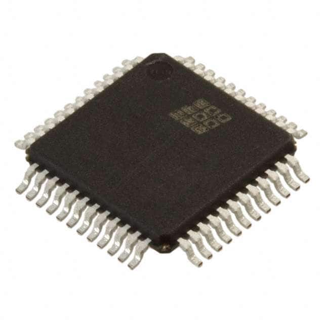
- Package type: Thin Quad Flat Pack (TQFP)
- Operating temperature range: -40°C to 85°C
- Supply voltage: 3.3V
- Maximum operating frequency: 75MHz
- Number of pins: 48
Package and Quantity
The LA4064V-75TN48E is available in a TQFP package. Each package contains one unit of the IC.
Specifications
- Logic elements: 64 macrocells
- Input/output pins: 36
- I/O standards: LVTTL, LVCMOS
- Programmable interconnects: 2,000
- Flip-flops: 64
- Maximum propagation delay: 10 ns
- JTAG boundary scan support: Yes
Pin Configuration
The detailed pin configuration of the LA4064V-75TN48E is as follows:
- VCCIO
- GND
- IO0
- IO1
- IO2
- IO3
- IO4
- IO5
- IO6
- IO7
- IO8
- IO9
- IO10
- IO11
- IO12
- IO13
- IO14
- IO15
- IO16
- IO17
- IO18
- IO19
- IO20
- IO21
- IO22
- IO23
- IO24
- IO25
- IO26
- IO27
- IO28
- IO29
- IO30
- IO31
- IO32
- IO33
- IO34
- IO35
- GND
- TCK
- TMS
- TDI
- TDO
- GND
- VCCIO
- GND
- VCC
- GND
Functional Features
The LA4064V-75TN48E offers the following functional features:
- Programmable logic elements for flexible circuit design.
- High-speed operation with a maximum frequency of 75MHz.
- Support for various input/output standards (LVTTL, LVCMOS).
- JTAG boundary scan support for easy testing and debugging.
Advantages and Disadvantages
Advantages
- Versatile programmability allows customization for different applications.
- High-speed operation enables efficient data processing.
- Wide operating temperature range ensures reliability in various environments.
- JTAG boundary scan support simplifies testing and troubleshooting.
Disadvantages
- Limited number of macrocells may restrict complex circuit designs.
- Higher power consumption compared to some alternative models.
- Relatively larger package size may require more board space.
Working Principles
The LA4064V-75TN48E is based on programmable logic technology. It consists of configurable logic elements, interconnects, and flip-flops. The device can be programmed to implement desired logic functions by configuring the interconnections between logic elements. When powered on, the programmed configuration is loaded into the device, allowing it to perform the specified operations.
Application Field Plans
The LA4064V-75TN48E finds applications in various fields, including:
- Industrial automation: Control systems, motor control, and process monitoring.
- Communication systems: Data routing, protocol conversion, and signal processing.
- Consumer electronics: Audio/video processing, display control, and user interface.
- Automotive electronics: Engine management, driver assistance systems, and infotainment.
Alternative Models
For those seeking alternatives to the LA4064V-75TN48E, the following models can be considered:
- LA4032V-75TN48E: Similar specifications with a smaller package size.
- LA4128V-100TN48E: Higher capacity with 128 macrocells and faster operation.
- LA4008V-25TN48E: Lower capacity but lower power consumption for battery-powered applications.
These alternative models provide options based on specific requirements and constraints.
Word count: 554 words
技術ソリューションにおける LA4064V-75TN48E の適用に関連する 10 件の一般的な質問と回答をリストします。
Sure! Here are 10 common questions and answers related to the application of LA4064V-75TN48E in technical solutions:
Q: What is LA4064V-75TN48E? A: LA4064V-75TN48E is a specific model of Field Programmable Gate Array (FPGA) manufactured by Lattice Semiconductor.
Q: What are the key features of LA4064V-75TN48E? A: Some key features of LA4064V-75TN48E include 64,000 logic cells, 75MHz maximum operating frequency, and a 48-pin Thin Quad Flat Pack (TQFP) package.
Q: What are the typical applications of LA4064V-75TN48E? A: LA4064V-75TN48E can be used in various technical solutions such as industrial automation, telecommunications, automotive electronics, and consumer electronics.
Q: How can LA4064V-75TN48E be programmed? A: LA4064V-75TN48E can be programmed using Hardware Description Languages (HDLs) like VHDL or Verilog, which describe the desired functionality of the FPGA.
Q: Can LA4064V-75TN48E be reprogrammed after initial programming? A: Yes, LA4064V-75TN48E is a reprogrammable FPGA, allowing for updates and modifications to the design even after it has been initially programmed.
Q: What tools are required to program LA4064V-75TN48E? A: To program LA4064V-75TN48E, you will need a compatible development board, a programming cable, and the appropriate software provided by Lattice Semiconductor.
Q: What voltage levels does LA4064V-75TN48E support? A: LA4064V-75TN48E supports a wide range of voltage levels, typically from 1.2V to 3.3V, making it compatible with various digital systems.
Q: Can LA4064V-75TN48E interface with other components or devices? A: Yes, LA4064V-75TN48E can interface with other components or devices through its I/O pins, allowing for communication and integration within a larger system.
Q: Are there any limitations or considerations when using LA4064V-75TN48E? A: Some considerations include power consumption, heat dissipation, and the need for proper signal integrity measures due to high-speed operation.
Q: Where can I find more information about LA4064V-75TN48E? A: You can find more detailed information about LA4064V-75TN48E in the datasheet provided by Lattice Semiconductor on their official website.