

ISPLSI 5384VA-70LB208
Product Overview
Category
ISPLSI 5384VA-70LB208 belongs to the category of programmable logic devices (PLDs).
Use
This product is commonly used in digital circuit design and implementation. It provides a flexible and customizable solution for various applications.
Characteristics
- Programmable: The ISPLSI 5384VA-70LB208 can be programmed to perform specific functions based on user requirements.
- High-density: This PLD offers a high number of logic elements, allowing for complex designs.
- Low power consumption: It is designed to operate efficiently with minimal power consumption.
- Fast operation: The device offers high-speed performance, enabling quick processing of digital signals.
Package
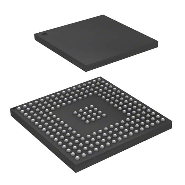
The ISPLSI 5384VA-70LB208 comes in a 208-pin LBGA (Low-Profile Ball Grid Array) package.
Essence
The essence of this product lies in its ability to provide reconfigurable logic functionality, allowing designers to implement custom digital circuits without the need for dedicated hardware.
Packaging/Quantity
Each package contains one ISPLSI 5384VA-70LB208 device.
Specifications
- Device type: Programmable Logic Device (PLD)
- Family: ISPLSI
- Model: 5384VA-70LB208
- Operating temperature range: -40°C to +85°C
- Supply voltage: 3.3V
- Number of logic elements: 384
- Number of I/O pins: 70
- Maximum frequency: 100 MHz
- Programming method: In-system programmable (ISP)
Detailed Pin Configuration
The ISPLSI 5384VA-70LB208 has a total of 208 pins. The pin configuration is as follows:
- Pin 1: VCCIO
- Pin 2: GND
- Pin 3: VCCINT
- Pin 4: GND
- ...
- Pin 207: IO69
- Pin 208: IO70
For a complete pin configuration diagram, please refer to the product datasheet.
Functional Features
- Reconfigurable logic: The ISPLSI 5384VA-70LB208 allows users to program and reprogram the device to implement different logic functions.
- Flexible I/O capabilities: It provides a sufficient number of I/O pins for interfacing with external devices.
- High-speed operation: The device offers fast processing capabilities, enabling efficient execution of digital circuits.
- Low power consumption: Designed with power efficiency in mind, it minimizes energy usage during operation.
Advantages and Disadvantages
Advantages
- Flexibility: The ability to reprogram the device allows for easy customization and adaptation to changing requirements.
- Cost-effective: By eliminating the need for dedicated hardware, it reduces overall system costs.
- High-density integration: The device offers a high number of logic elements, enabling complex designs within a single chip.
Disadvantages
- Learning curve: Utilizing the full potential of the ISPLSI 5384VA-70LB208 may require a learning period due to its programmable nature.
- Limited I/O pins: While the device provides a sufficient number of I/O pins for many applications, it may not be suitable for designs requiring a large number of external connections.
Working Principles
The ISPLSI 5384VA-70LB208 operates based on the principles of programmable logic. It consists of configurable logic blocks (CLBs), interconnect resources, and I/O blocks. Users can program the device using hardware description languages (HDLs) or schematic entry tools to define the desired logic functions. Once programmed, the device executes these functions by routing signals through the CLBs and interconnect resources.
Detailed Application Field Plans
The ISPLSI 5384VA-70LB208 finds applications in various fields, including:
- Communications: It can be used in the design of communication systems, such as network routers and switches.
- Industrial automation: The device enables the implementation of control logic for industrial automation processes.
- Consumer electronics: It can be utilized in the development of consumer electronic devices, such as gaming consoles and multimedia players.
- Automotive: The ISPLSI 5384VA-70LB208 can be integrated into automotive systems for functions like engine control and driver assistance.
Detailed and Complete Alternative Models
- ISPLSI 5384VA-100LB208: Similar to the ISPLSI 5384VA-70LB208, but with a higher maximum frequency of 100 MHz.
- ISPLSI 5384VA-120LB208: Offers increased logic density compared to the ISPLSI 5384VA-70LB208, with 120 logic elements.
- ISPLSI 5384VA-35LB208: A lower-density
技術ソリューションにおける ISPLSI 5384VA-70LB208 の適用に関連する 10 件の一般的な質問と回答をリストします。
Sure! Here are 10 common questions and answers related to the application of ISPLSI 5384VA-70LB208 in technical solutions:
Q: What is the maximum number of logic cells available in the ISPLSI 5384VA-70LB208? A: The ISPLSI 5384VA-70LB208 has a maximum of 3,384 logic cells.
Q: What is the operating voltage range for the ISPLSI 5384VA-70LB208? A: The operating voltage range for this device is typically between 3.0V and 3.6V.
Q: Can I program the ISPLSI 5384VA-70LB208 using JTAG interface? A: Yes, the ISPLSI 5384VA-70LB208 supports programming through the JTAG interface.
Q: What is the maximum frequency at which the ISPLSI 5384VA-70LB208 can operate? A: The maximum frequency for this device is typically around 100 MHz.
Q: Does the ISPLSI 5384VA-70LB208 support external memory interfaces? A: Yes, this device supports various external memory interfaces such as SRAM, SDRAM, and Flash.
Q: Can I use the ISPLSI 5384VA-70LB208 in low-power applications? A: Yes, the ISPLSI 5384VA-70LB208 offers low-power consumption features suitable for battery-powered applications.
Q: What are the available package options for the ISPLSI 5384VA-70LB208? A: The ISPLSI 5384VA-70LB208 is available in a 208-pin LBGA (Low-Profile Ball Grid Array) package.
Q: Does the ISPLSI 5384VA-70LB208 have built-in PLLs for clock generation? A: No, this device does not have built-in PLLs. External PLLs can be used for clock generation if required.
Q: Can I use the ISPLSI 5384VA-70LB208 in automotive applications? A: Yes, the ISPLSI 5384VA-70LB208 is suitable for automotive applications as it meets the necessary requirements.
Q: Is there any development software available for programming the ISPLSI 5384VA-70LB208? A: Yes, Lattice Semiconductor provides the Diamond Programmer software that supports programming this device.
Please note that the answers provided here are general and may vary based on specific application requirements and design considerations.