

EP4CGX75DF27C8N
Product Overview
Category: Integrated Circuit (IC)
Use: The EP4CGX75DF27C8N is a programmable logic device (PLD) that belongs to the Cyclone IV GX family of FPGAs (Field-Programmable Gate Arrays). It is designed for high-performance applications that require flexibility and reconfigurability.
Characteristics: - High-density FPGA with 75,000 logic elements - Low power consumption - High-speed performance - Built-in memory blocks and digital signal processing (DSP) capabilities - Support for various I/O standards - Flexible configuration options
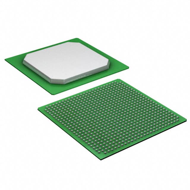
Package: The EP4CGX75DF27C8N comes in a compact 27x27 mm package, making it suitable for space-constrained designs.
Essence: This PLD offers designers the ability to implement complex digital circuits and systems on a single chip. Its reprogrammable nature allows for easy updates and modifications during the development and production stages.
Packaging/Quantity: The EP4CGX75DF27C8N is typically sold in trays or reels, with quantities varying depending on the supplier and customer requirements.
Specifications
- Logic Elements: 75,000
- Embedded Memory: Up to 3.9 Mb
- DSP Blocks: 288
- Maximum User I/Os: 622
- Operating Voltage: 1.2V
- Operating Temperature Range: -40°C to 100°C
- Package Type: FBGA (Fine-Pitch Ball Grid Array)
- Package Pins: 780
Detailed Pin Configuration
The EP4CGX75DF27C8N has a total of 780 pins, which are assigned to various functions such as input/output, clock signals, power supply, and configuration. For a detailed pin configuration diagram, please refer to the manufacturer's datasheet.
Functional Features
- High-speed performance: The EP4CGX75DF27C8N operates at high clock frequencies, enabling rapid data processing and real-time applications.
- Flexible I/O standards: It supports a wide range of I/O standards, allowing seamless integration with different devices and interfaces.
- Built-in memory blocks: The embedded memory blocks provide efficient storage for data-intensive applications, reducing the need for external memory components.
- Digital signal processing (DSP) capabilities: The FPGA includes dedicated DSP blocks that enable efficient implementation of complex mathematical operations.
- Reconfigurability: The EP4CGX75DF27C8N can be reprogrammed multiple times, allowing designers to adapt and optimize their designs as needed.
Advantages and Disadvantages
Advantages: - High-density FPGA with ample logic elements for complex designs - Low power consumption, making it suitable for battery-powered applications - Support for various I/O standards enhances compatibility - Built-in memory blocks and DSP capabilities reduce the need for additional components - Reprogrammable nature allows for design flexibility and updates
Disadvantages: - Limited availability of alternative models with similar specifications - Higher cost compared to lower-end FPGAs - Steeper learning curve for beginners due to its advanced features
Working Principles
The EP4CGX75DF27C8N is based on the concept of programmable logic. It consists of an array of configurable logic blocks (CLBs) interconnected through programmable routing resources. These CLBs can be programmed to implement desired logic functions, creating custom digital circuits.
During operation, the FPGA is configured by loading a bitstream into its internal memory. This bitstream defines the interconnections and functionality of the logic elements within the device. Once configured, the FPGA performs the desired operations based on the programmed logic.
Detailed Application Field Plans
The EP4CGX75DF27C8N finds applications in various fields, including but not limited to: - Telecommunications: Used in base stations, network switches, and routers for high-speed data processing and signal routing. - Industrial Automation: Enables real-time control and monitoring of complex systems, such as robotics and manufacturing equipment. - Aerospace and Defense: Utilized in avionics systems, radar signal processing, and secure communications. - Medical Devices: Supports advanced imaging, signal processing, and patient monitoring applications. - Automotive: Enables advanced driver assistance systems (ADAS), infotainment systems, and engine control units (ECUs).
Alternative Models
While the EP4CGX75DF27C8N offers a unique combination of features, there are alternative models available from other FPGA manufacturers. Some notable alternatives include: - Xilinx Virtex-7 series - Intel Stratix IV series - LatticeECP5 series
These alternative models offer similar capabilities and can be considered based on specific project requirements and compatibility considerations.
In conclusion, the EP4CGX75DF27C8N
技術ソリューションにおける EP4CGX75DF27C8N の適用に関連する 10 件の一般的な質問と回答をリストします。
Sure! Here are 10 common questions and answers related to the application of EP4CGX75DF27C8N in technical solutions:
1. What is EP4CGX75DF27C8N? EP4CGX75DF27C8N is a field-programmable gate array (FPGA) manufactured by Intel. It is part of the Cyclone IV GX series and offers a range of features for implementing complex digital designs.
2. What are the key features of EP4CGX75DF27C8N? Some key features of EP4CGX75DF27C8N include 75,000 logic elements, 4-phase locked loops (PLLs), embedded memory blocks, high-speed transceivers, and support for various I/O standards.
3. What are the typical applications of EP4CGX75DF27C8N? EP4CGX75DF27C8N can be used in a wide range of applications such as telecommunications, industrial automation, automotive systems, video processing, medical devices, and more.
4. How can EP4CGX75DF27C8N be programmed? EP4CGX75DF27C8N can be programmed using Intel's Quartus Prime software, which provides a user-friendly interface for designing, simulating, and programming FPGA designs.
5. Can EP4CGX75DF27C8N be used for high-speed data processing? Yes, EP4CGX75DF27C8N is equipped with high-speed transceivers that support various protocols like PCIe, Gigabit Ethernet, and USB. This makes it suitable for applications requiring high-speed data processing.
6. Does EP4CGX75DF27C8N support external memory interfaces? Yes, EP4CGX75DF27C8N supports various external memory interfaces such as DDR3, DDR2, and QDR II+. This allows for efficient data storage and retrieval in FPGA-based designs.
7. Can EP4CGX75DF27C8N interface with other devices or microcontrollers? Yes, EP4CGX75DF27C8N supports various communication protocols like SPI, I2C, UART, and GPIOs, enabling it to interface with other devices or microcontrollers in a system.
8. What are the power requirements for EP4CGX75DF27C8N? The power requirements for EP4CGX75DF27C8N vary depending on the design and configuration. It typically operates at a voltage range of 1.15V to 1.25V.
9. Is EP4CGX75DF27C8N suitable for low-power applications? EP4CGX75DF27C8N is not specifically designed for low-power applications. However, by optimizing the design and utilizing power-saving techniques, it can be used in low-power systems.
10. Are there any development boards available for EP4CGX75DF27C8N? Yes, Intel provides development boards like the Cyclone IV GX Starter Kit, which includes EP4CGX75DF27C8N. These boards offer a platform for prototyping and testing FPGA designs.
Please note that the specific details and answers may vary based on the manufacturer's documentation and specifications.