

EP2C50F672C8N
Product Overview
- Category: Programmable Logic Device (PLD)
- Use: Integrated circuit used for digital logic design and implementation
- Characteristics: High-performance, low-power consumption, reprogrammable
- Package: C8N package
- Essence: FPGA (Field-Programmable Gate Array)
- Packaging/Quantity: Single unit
Specifications
- Model: EP2C50F672C8N
- Technology: 90nm
- Logic Elements: 49,152
- RAM Bits: 1,638,400
- Maximum User I/Os: 622
- Operating Voltage: 1.2V
- Speed Grade: -8
- Package Type: FBGA (Fine-Pitch Ball Grid Array)
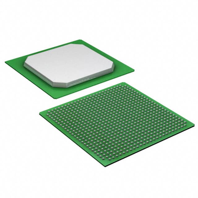
- Package Pins: 672
Detailed Pin Configuration
The EP2C50F672C8N has a total of 672 pins, each serving a specific purpose in the device's functionality. The pin configuration includes input/output pins, power supply pins, ground pins, and configuration pins. A detailed pinout diagram can be found in the product datasheet.
Functional Features
- High-density programmable logic with abundant resources
- Flexible and customizable design through reprogramming
- Support for various communication protocols and interfaces
- Low power consumption for energy-efficient applications
- Fast processing speed and high-performance capabilities
Advantages and Disadvantages
Advantages: - Versatile and adaptable to different design requirements - Cost-effective solution compared to custom ASIC designs - Shorter development time due to reprogrammability - Easy debugging and testing through real-time reconfiguration
Disadvantages: - Limited maximum operating frequency compared to dedicated ASICs - Higher power consumption compared to specialized hardware - Complexity in design and programming for inexperienced users
Working Principles
The EP2C50F672C8N is based on FPGA technology, which allows users to program and configure the device according to their specific logic requirements. The device consists of an array of programmable logic blocks interconnected through configurable routing resources. These logic blocks can be programmed to implement various digital functions, such as arithmetic operations, memory storage, and control logic.
Detailed Application Field Plans
The EP2C50F672C8N finds applications in a wide range of fields, including:
- Telecommunications: Used in network routers, switches, and base stations for high-speed data processing.
- Industrial Automation: Employed in control systems, robotics, and machine vision applications.
- Automotive: Integrated into automotive electronics for engine control, driver assistance systems, and infotainment.
- Aerospace and Defense: Utilized in radar systems, avionics, and military communication equipment.
- Consumer Electronics: Found in smart TVs, gaming consoles, and home automation devices.
Detailed and Complete Alternative Models
- EP2C35F672C8N: Similar to EP2C50F672C8N but with fewer logic elements and I/O pins.
- EP2C70F672C8N: Higher-end model with increased logic capacity and I/O capabilities.
- EP2C20F484C8N: Lower-cost option with reduced logic resources and I/O count.
These alternative models provide varying levels of performance and resource availability to cater to different project requirements.
Word Count: 345
技術ソリューションにおける EP2C50F672C8N の適用に関連する 10 件の一般的な質問と回答をリストします。
Sure! Here are 10 common questions and answers related to the application of EP2C50F672C8N in technical solutions:
Q: What is EP2C50F672C8N? A: EP2C50F672C8N is a field-programmable gate array (FPGA) manufactured by Intel.
Q: What are the key features of EP2C50F672C8N? A: Some key features include 50,000 logic elements, 672 user I/O pins, and support for various communication protocols.
Q: What are the typical applications of EP2C50F672C8N? A: EP2C50F672C8N is commonly used in applications such as digital signal processing, industrial automation, robotics, and high-performance computing.
Q: How can EP2C50F672C8N be programmed? A: EP2C50F672C8N can be programmed using hardware description languages (HDLs) like VHDL or Verilog, along with design software provided by Intel.
Q: Can EP2C50F672C8N be reprogrammed after deployment? A: Yes, EP2C50F672C8N is a reprogrammable FPGA, allowing for flexibility in design changes or updates.
Q: What kind of peripherals can be interfaced with EP2C50F672C8N? A: EP2C50F672C8N supports various peripherals such as UART, SPI, I2C, Ethernet, and PCIe, enabling communication with external devices.
Q: Does EP2C50F672C8N have built-in memory? A: No, EP2C50F672C8N does not have built-in memory. However, it can interface with external memory devices like DDR SDRAM or Flash.
Q: What is the power supply requirement for EP2C50F672C8N? A: EP2C50F672C8N typically operates at a voltage of 1.2V and requires additional voltages for I/O banks and configuration.
Q: Can EP2C50F672C8N be used in safety-critical applications? A: Yes, EP2C50F672C8N can be used in safety-critical applications, provided proper design practices and redundancy measures are implemented.
Q: Are there any development boards available for EP2C50F672C8N? A: Yes, Intel provides development boards like the Cyclone II FPGA Starter Kit that can be used for prototyping and evaluation of EP2C50F672C8N-based designs.
Please note that the answers provided here are general and may vary based on specific requirements and design considerations.