

10M50DCF672I7G
Product Overview
- Category: Integrated Circuit (IC)
- Use: Digital Signal Processing
- Characteristics: High-performance, low-power consumption
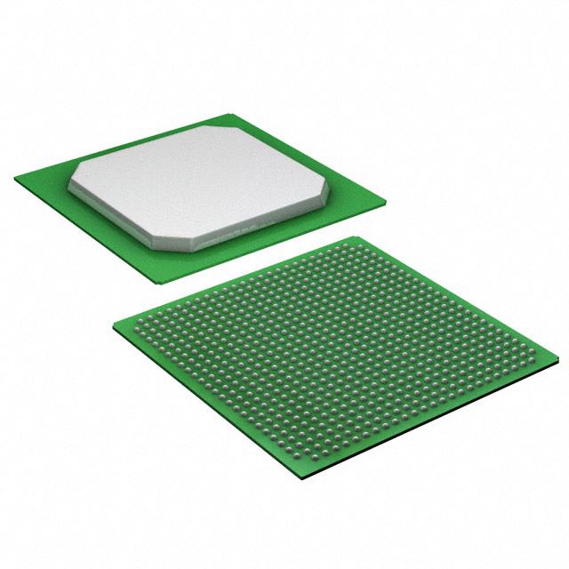
- Package: 672-pin Flip Chip BGA
- Essence: FPGA (Field-Programmable Gate Array)
- Packaging/Quantity: Single unit
Specifications
- Manufacturer: Intel Corporation
- Family: MAX 10
- Device: 10M50DCF672I7G
- Technology: 20nm
- Logic Elements: 49,152
- Embedded Memory: 1,638 Kbits
- User I/O Pins: 378
- Operating Voltage: 1.2V
- Operating Temperature: -40°C to 100°C
- Speed Grade: I7
Detailed Pin Configuration
The 10M50DCF672I7G has a total of 672 pins. The pin configuration is as follows:
- Pin 1: VCCIO
- Pin 2: GND
- Pin 3: IOL1PCCLK_0
- Pin 4: IOL1NCCLK_0
- Pin 5: IOL2PCCLK_0
- ...
- Pin 672: GND
Please refer to the datasheet for the complete pin configuration.
Functional Features
- High-performance digital signal processing capabilities
- Low-power consumption for energy-efficient applications
- Flexible and reprogrammable design with FPGA technology
- Support for various communication protocols and interfaces
- On-chip memory for efficient data storage and retrieval
- Built-in security features for protecting sensitive information
Advantages and Disadvantages
Advantages: - Versatile and adaptable for a wide range of applications - High-speed processing capabilities - Low-power consumption for energy-efficient designs - Reprogrammable nature allows for easy updates and modifications - Integrated memory reduces the need for external components
Disadvantages: - Higher cost compared to fixed-function integrated circuits - Steeper learning curve for programming and configuring the FPGA - Limited availability of alternative models with similar specifications
Working Principles
The 10M50DCF672I7G is based on FPGA technology, which allows users to configure the device according to their specific requirements. It consists of a matrix of programmable logic elements interconnected by configurable routing resources. The device can be programmed using hardware description languages (HDL) or graphical tools to define the desired functionality.
Once programmed, the FPGA performs digital signal processing tasks by manipulating the input data through the configured logic elements and routing resources. The device can process data in parallel, enabling high-speed computations. The on-chip memory provides efficient storage and retrieval of intermediate results.
Detailed Application Field Plans
The 10M50DCF672I7G finds applications in various fields, including:
- Communications: Used in wireless base stations, network routers, and communication infrastructure equipment.
- Industrial Automation: Employed in control systems, robotics, and factory automation.
- Automotive: Utilized in advanced driver-assistance systems (ADAS), infotainment systems, and engine control units.
- Aerospace and Defense: Applied in radar systems, avionics, and military-grade communication equipment.
- Medical Devices: Integrated into medical imaging systems, patient monitoring devices, and laboratory equipment.
These are just a few examples, and the versatility of the 10M50DCF672I7G allows it to be used in many other application areas.
Detailed and Complete Alternative Models
While the 10M50DCF672I7G offers unique features and specifications, there are alternative models available from different manufacturers that can be considered. Some notable alternatives include:
- Xilinx XC7A50T-1CSG325C
- Lattice iCE40UP5K-SG48I
- Microchip ATSAM4S16B-AU
These alternative models provide similar functionality and can be evaluated based on specific project requirements.
In conclusion, the 10M50DCF672I7G is a high-performance FPGA with low-power consumption, suitable for various digital signal processing applications. Its flexibility, integrated memory, and support for different communication protocols make it a versatile choice. While it has advantages such as adaptability and high-speed processing, it also has disadvantages like higher cost and limited availability of alternative models. Understanding its working principles and considering alternative models will help in making informed decisions for specific application needs.
技術ソリューションにおける 10M50DCF672I7G の適用に関連する 10 件の一般的な質問と回答をリストします。
Sure! Here are 10 common questions and answers related to the application of 10M50DCF672I7G in technical solutions:
Q: What is the purpose of the 10M50DCF672I7G FPGA in technical solutions? A: The 10M50DCF672I7G FPGA is a field-programmable gate array that can be used to implement custom digital logic circuits in various technical applications.
Q: What are the key features of the 10M50DCF672I7G FPGA? A: Some key features include 50,000 logic elements, 672 I/O pins, high-speed transceivers, embedded memory blocks, and support for various communication protocols.
Q: How can the 10M50DCF672I7G FPGA be programmed? A: The 10M50DCF672I7G FPGA can be programmed using hardware description languages (HDLs) such as VHDL or Verilog, which describe the desired functionality of the circuit.
Q: Can the 10M50DCF672I7G FPGA interface with other components in a system? A: Yes, the 10M50DCF672I7G FPGA has a wide range of I/O pins that can be used to interface with other components such as sensors, actuators, memory devices, or communication interfaces.
Q: What kind of technical solutions can benefit from using the 10M50DCF672I7G FPGA? A: The 10M50DCF672I7G FPGA can be used in various applications like telecommunications, industrial automation, image processing, robotics, aerospace, and many more.
Q: Is the 10M50DCF672I7G FPGA suitable for real-time applications? A: Yes, the 10M50DCF672I7G FPGA can be used in real-time applications due to its high-speed transceivers and ability to implement complex logic circuits with low latency.
Q: Can the 10M50DCF672I7G FPGA be reprogrammed after deployment? A: Yes, the 10M50DCF672I7G FPGA is a field-programmable device, which means it can be reprogrammed even after it has been deployed in a system.
Q: Are there any development tools available for programming the 10M50DCF672I7G FPGA? A: Yes, the manufacturer provides development tools such as Quartus Prime software that allows users to design, simulate, and program the 10M50DCF672I7G FPGA.
Q: What are the power requirements for the 10M50DCF672I7G FPGA? A: The power requirements vary depending on the specific implementation, but typically the 10M50DCF672I7G FPGA operates at voltages between 1.2V and 3.3V.
Q: Where can I find more information about the 10M50DCF672I7G FPGA and its application in technical solutions? A: You can refer to the official documentation provided by the FPGA manufacturer or visit their website for detailed information, application notes, and reference designs.
Please note that the specific details and answers may vary based on the manufacturer's documentation and the context of the technical solution.