

1EDN7512GXTMA1
Product Overview
Category
1EDN7512GXTMA1 belongs to the category of high-speed, low-side gate drivers.
Use
This product is primarily used for driving power MOSFETs and IGBTs in various applications such as motor control, power supplies, and inverters.
Characteristics
- High-speed switching capability
- Low input/output capacitance
- Wide operating voltage range
- Integrated protection features (e.g., undervoltage lockout, overtemperature shutdown)
- Compact package size for space-constrained designs
Package
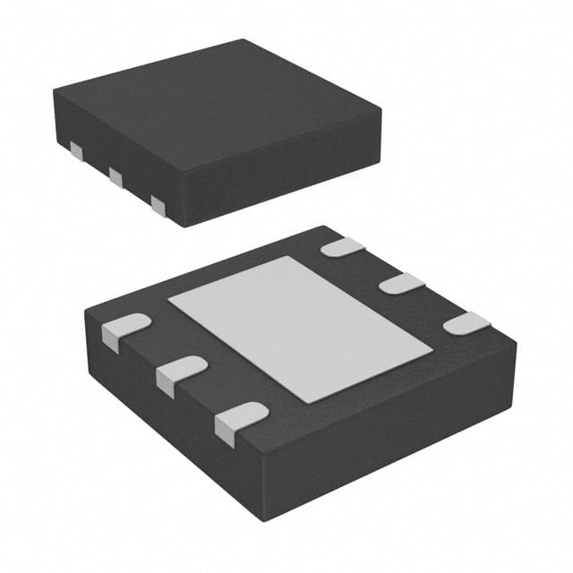
1EDN7512GXTMA1 is available in a small surface-mount package, allowing for easy integration into electronic circuits.
Essence
The essence of 1EDN7512GXTMA1 lies in its ability to provide efficient and reliable gate driving for power semiconductor devices, enabling optimal performance and protection.
Packaging/Quantity
This product is typically packaged in reels or tubes, with a quantity of 250 units per reel/tube.
Specifications
- Supply Voltage: 4.5V to 18V
- Output Current: 2A
- Propagation Delay: <100ns
- Operating Temperature Range: -40°C to +125°C
- Isolation Voltage: 2500Vrms
Detailed Pin Configuration
1EDN7512GXTMA1 has the following pin configuration:
- VCC: Power supply input
- IN: Input control signal
- GND: Ground reference
- OUT: Gate driver output
Functional Features
- High-speed switching: Enables fast and precise control of power semiconductor devices.
- Integrated protection: Safeguards against potential faults and abnormal operating conditions.
- Low input/output capacitance: Reduces power losses and improves efficiency.
- Wide operating voltage range: Provides flexibility in various applications.
- Compact size: Facilitates space-saving designs.
Advantages and Disadvantages
Advantages
- High-speed switching capability enhances system performance.
- Integrated protection features improve reliability and safety.
- Low input/output capacitance reduces power losses.
- Wide operating voltage range allows for versatile application possibilities.
- Compact package size enables space-constrained designs.
Disadvantages
- Limited output current may not be suitable for high-power applications.
- Requires external components for proper operation.
- Higher cost compared to traditional gate drivers.
Working Principles
1EDN7512GXTMA1 operates by receiving an input control signal (IN) and generating a corresponding output voltage (OUT) to drive the gate of a power MOSFET or IGBT. The integrated circuitry ensures precise timing, voltage levels, and protection mechanisms to optimize the performance and reliability of the driven device.
Detailed Application Field Plans
1EDN7512GXTMA1 finds applications in various fields, including:
- Motor Control: Enables efficient and precise control of motor speed and direction in electric vehicles, industrial machinery, and robotics.
- Power Supplies: Facilitates reliable and stable power conversion in AC/DC and DC/DC converters.
- Inverters: Enhances the efficiency and performance of inverters used in renewable energy systems, such as solar and wind power.
Detailed and Complete Alternative Models
- 1EDN7510GXTMA1
- 1EDN7511GXTMA1
- 1EDN7513GXTMA1
- 1EDN7514GXTMA1
These alternative models offer similar functionality and characteristics, providing options for different design requirements.
Word count: 511 words
技術ソリューションにおける 1EDN7512GXTMA1 の適用に関連する 10 件の一般的な質問と回答をリストします。
Sure! Here are 10 common questions and answers related to the application of 1EDN7512GXTMA1 in technical solutions:
Q1: What is the 1EDN7512GXTMA1? A1: The 1EDN7512GXTMA1 is a high-speed, dual-channel gate driver IC designed for driving MOSFETs and IGBTs in various power electronics applications.
Q2: What is the maximum voltage rating of the 1EDN7512GXTMA1? A2: The maximum voltage rating of the 1EDN7512GXTMA1 is typically around 600V.
Q3: What is the output current capability of the 1EDN7512GXTMA1? A3: The 1EDN7512GXTMA1 can provide a peak output current of up to 4A.
Q4: Can the 1EDN7512GXTMA1 be used with both MOSFETs and IGBTs? A4: Yes, the 1EDN7512GXTMA1 is compatible with both MOSFETs and IGBTs, making it versatile for different power electronics applications.
Q5: Does the 1EDN7512GXTMA1 have built-in protection features? A5: Yes, the 1EDN7512GXTMA1 includes various protection features such as under-voltage lockout (UVLO), over-temperature protection (OTP), and short-circuit protection (SCP).
Q6: What is the operating temperature range of the 1EDN7512GXTMA1? A6: The 1EDN7512GXTMA1 has an operating temperature range of -40°C to +125°C.
Q7: Can the 1EDN7512GXTMA1 be used in high-frequency applications? A7: Yes, the 1EDN7512GXTMA1 is designed for high-speed operation and can be used in high-frequency applications.
Q8: What is the typical input voltage range of the 1EDN7512GXTMA1? A8: The typical input voltage range of the 1EDN7512GXTMA1 is between 4.5V and 20V.
Q9: Does the 1EDN7512GXTMA1 require an external bootstrap diode? A9: No, the 1EDN7512GXTMA1 has an integrated bootstrap diode, simplifying the design and reducing component count.
Q10: Can the 1EDN7512GXTMA1 be used in automotive applications? A10: Yes, the 1EDN7512GXTMA1 meets the requirements for automotive applications and is suitable for use in automotive systems.
Please note that the answers provided here are general and may vary depending on specific application requirements. It is always recommended to refer to the datasheet and consult with the manufacturer for detailed information.