

IDT74SSTVN16859PAG8
Basic Information Overview
- Category: Integrated Circuit (IC)
- Use: Signal Voltage Translator
- Characteristics: High-speed, low-power, bidirectional voltage translation
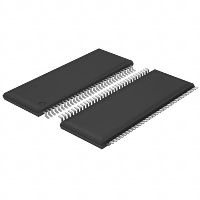
- Package: 56-pin TSSOP (Thin Shrink Small Outline Package)
- Essence: Translates signals between different voltage levels
- Packaging/Quantity: Tape and reel packaging, 250 units per reel
Specifications
- Supply Voltage Range: 1.2V to 3.6V
- Input Voltage Range: 0V to VCC
- Output Voltage Range: 0V to VCC
- Maximum Data Rate: 400 Mbps
- Operating Temperature Range: -40°C to +85°C
Detailed Pin Configuration
The IDT74SSTVN16859PAG8 has a total of 56 pins, which are assigned specific functions. The pin configuration is as follows:
- OE (Output Enable) A1
- GND (Ground) A2
- VCC (Supply Voltage) A3
- A Port 0 (Input/Output) A4
- A Port 1 (Input/Output) A5
- A Port 2 (Input/Output) A6
- A Port 3 (Input/Output) A7
- A Port 4 (Input/Output) A8
- A Port 5 (Input/Output) A9
- A Port 6 (Input/Output) A10
- A Port 7 (Input/Output) A11
- A Port 8 (Input/Output) A12
- A Port 9 (Input/Output) A13
- A Port 10 (Input/Output) A14
- A Port 11 (Input/Output) A15
- A Port 12 (Input/Output) A16
- A Port 13 (Input/Output) A17
- A Port 14 (Input/Output) A18
- A Port 15 (Input/Output) A19
- VREF (Reference Voltage) A20
- GND (Ground) A21
- B Port 0 (Input/Output) A22
- B Port 1 (Input/Output) A23
- B Port 2 (Input/Output) A24
- B Port 3 (Input/Output) A25
- B Port 4 (Input/Output) A26
- B Port 5 (Input/Output) A27
- B Port 6 (Input/Output) A28
- B Port 7 (Input/Output) A29
- B Port 8 (Input/Output) A30
- B Port 9 (Input/Output) A31
- B Port 10 (Input/Output) A32
- B Port 11 (Input/Output) A33
- B Port 12 (Input/Output) A34
- B Port 13 (Input/Output) A35
- B Port 14 (Input/Output) A36
- B Port 15 (Input/Output) A37
- VREF (Reference Voltage) A38
- GND (Ground) A39
- VCC (Supply Voltage) A40
- OE (Output Enable) B1
- GND (Ground) B2
- VCC (Supply Voltage) B3
- B Port 0 (Input/Output) B4
- B Port 1 (Input/Output) B5
- B Port 2 (Input/Output) B6
- B Port 3 (Input/Output) B7
- B Port 4 (Input/Output) B8
- B Port 5 (Input/Output) B9
- B Port 6 (Input/Output) B10
- B Port 7 (Input/Output) B11
- B Port 8 (Input/Output) B12
- B Port 9 (Input/Output) B13
- B Port 10 (Input/Output) B14
- B Port 11 (Input/Output) B15
- VCC (Supply Voltage) B16
Functional Features
- Bidirectional voltage translation between two different voltage domains
- Supports high-speed data transmission up to 400 Mbps
- Low-power consumption for energy-efficient operation
- Automatic direction control for simplified interface design
- Provides voltage level shifting for compatibility between different logic families
Advantages and Disadv
技術ソリューションにおける IDT74SSTVN16859PAG8 の適用に関連する 10 件の一般的な質問と回答をリストします。
Sure! Here are 10 common questions and answers related to the application of IDT74SSTVN16859PAG8 in technical solutions:
Question: What is the IDT74SSTVN16859PAG8?
Answer: The IDT74SSTVN16859PAG8 is a high-performance 20-bit registered buffer with voltage translation capabilities.Question: What is the voltage translation range of the IDT74SSTVN16859PAG8?
Answer: The IDT74SSTVN16859PAG8 supports voltage translation from 1.2V to 3.3V.Question: What is the maximum data rate supported by the IDT74SSTVN16859PAG8?
Answer: The IDT74SSTVN16859PAG8 can support data rates up to 400 Mbps.Question: Can the IDT74SSTVN16859PAG8 be used for level shifting between different voltage domains?
Answer: Yes, the IDT74SSTVN16859PAG8 is specifically designed for voltage level shifting applications.Question: How many input/output (I/O) pins does the IDT74SSTVN16859PAG8 have?
Answer: The IDT74SSTVN16859PAG8 has a total of 20 I/O pins.Question: Does the IDT74SSTVN16859PAG8 have any built-in ESD protection?
Answer: Yes, the IDT74SSTVN16859PAG8 features built-in ESD protection on all I/O pins.Question: Can the IDT74SSTVN16859PAG8 be used in both uni-directional and bi-directional applications?
Answer: Yes, the IDT74SSTVN16859PAG8 can be used in both uni-directional and bi-directional voltage translation scenarios.Question: What is the power supply voltage range for the IDT74SSTVN16859PAG8?
Answer: The IDT74SSTVN16859PAG8 operates with a power supply voltage range of 1.2V to 3.6V.Question: Does the IDT74SSTVN16859PAG8 support hot insertion and removal of devices?
Answer: Yes, the IDT74SSTVN16859PAG8 is designed to support hot insertion and removal without causing any damage.Question: Can the IDT74SSTVN16859PAG8 be used in high-speed data communication applications?
Answer: Yes, the IDT74SSTVN16859PAG8 is suitable for high-speed data communication applications such as PCIe, SATA, USB, and more.
Please note that these answers are general and may vary depending on the specific application and requirements.