

IDT74SSTVN16859NLG8
Basic Information Overview
- Category: Integrated Circuit (IC)
- Use: Signal Voltage Translator
- Characteristics: High-speed, low-voltage, non-inverting translator
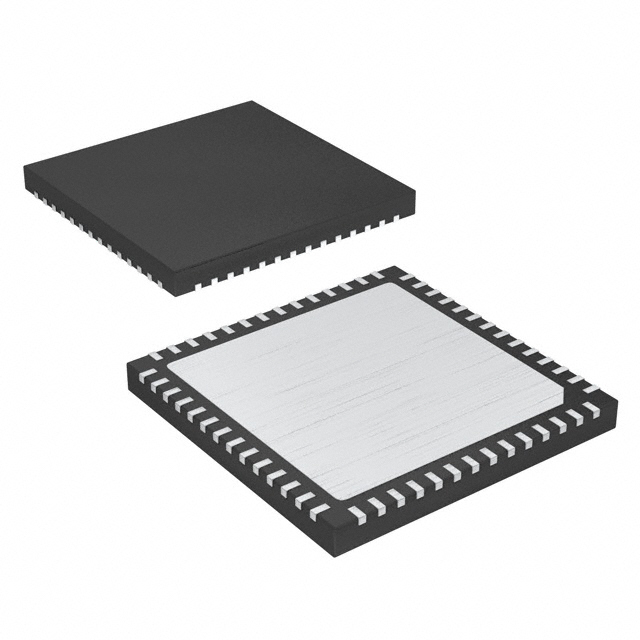
- Package: 56-pin QFN (Quad Flat No-Lead)
- Essence: Translates signals between different voltage levels
- Packaging/Quantity: Tape and Reel, 250 units per reel
Specifications
- Supply Voltage Range: 1.2V to 3.6V
- Input Voltage Range: 0V to VCC
- Output Voltage Range: 0V to VCC
- Maximum Data Rate: 400 Mbps
- Operating Temperature Range: -40°C to +85°C
Detailed Pin Configuration
The IDT74SSTVN16859NLG8 has a total of 56 pins. The pin configuration is as follows:
- VCCA - Positive supply voltage for Channel A
- GND - Ground
- A1 - Channel A input
- A2 - Channel A input
- A3 - Channel A input
- A4 - Channel A input
- A5 - Channel A input
- A6 - Channel A input
- A7 - Channel A input
- A8 - Channel A input
- A9 - Channel A input
- A10 - Channel A input
- A11 - Channel A input
- A12 - Channel A input
- A13 - Channel A input
- A14 - Channel A input
- A15 - Channel A input
- A16 - Channel A input
- VCCB - Positive supply voltage for Channel B
- B1 - Channel B input
- B2 - Channel B input
- B3 - Channel B input
- B4 - Channel B input
- B5 - Channel B input
- B6 - Channel B input
- B7 - Channel B input
- B8 - Channel B input
- B9 - Channel B input
- B10 - Channel B input
- B11 - Channel B input
- B12 - Channel B input
- B13 - Channel B input
- B14 - Channel B input
- B15 - Channel B input
- B16 - Channel B input
- OEAB - Output Enable for Channel A and B
- VREF - Reference Voltage
- GND - Ground
- Y1 - Channel A output
- Y2 - Channel A output
- Y3 - Channel A output
- Y4 - Channel A output
- Y5 - Channel A output
- Y6 - Channel A output
- Y7 - Channel A output
- Y8 - Channel A output
- Y9 - Channel A output
- Y10 - Channel A output
- Y11 - Channel A output
- Y12 - Channel A output
- Y13 - Channel A output
- Y14 - Channel A output
- Y15 - Channel A output
- Y16 - Channel A output
- GND - Ground
- VCCY - Positive supply voltage for Channel A outputs
Functional Features
- Non-inverting translation between two different voltage levels
- High-speed operation with a maximum data rate of 400 Mbps
- Supports bidirectional signal translation
- Low-voltage operation from 1.2V to 3.6V
- Provides voltage level shifting for various applications
Advantages and Disadvantages
Advantages: - High-speed operation allows for fast data transmission - Wide supply voltage range enables compatibility with different systems - Bidirectional translation simplifies signal routing in complex designs
Disadvantages: - Limited to non-inverting translation, may not be suitable for all applications requiring level shifting - Requires careful consideration of input and output voltage levels to ensure proper functionality
Working Principles
The IDT74SSTVN16859NLG8 is a signal voltage translator that operates by receiving input signals from Channel A and translating them to the corresponding voltage levels on Channel B. The translation is non-inverting, meaning that the logic levels are preserved during the translation process. The device uses internal circuitry to perform the voltage level shifting, allowing for seamless communication between systems operating at different voltage levels.
Detailed Application Field Plans
The IDT74SSTVN16859NLG8 can be used in various applications where voltage level translation is required. Some potential application fields include: - Communication systems - Data acquisition systems - Industrial automation - Automotive electronics - Consumer electronics
Detailed and Complete Alternative Models
- SN
技術ソリューションにおける IDT74SSTVN16859NLG8 の適用に関連する 10 件の一般的な質問と回答をリストします。
Sure! Here are 10 common questions and answers related to the application of IDT74SSTVN16859NLG8 in technical solutions:
Question: What is the IDT74SSTVN16859NLG8?
Answer: The IDT74SSTVN16859NLG8 is a high-performance 13-bit registered buffer with output enable.Question: What is the purpose of the IDT74SSTVN16859NLG8?
Answer: It is used to provide buffering and signal conditioning for digital signals in various technical applications.Question: What voltage levels does the IDT74SSTVN16859NLG8 support?
Answer: It supports both TTL (Transistor-Transistor Logic) and CMOS (Complementary Metal-Oxide-Semiconductor) voltage levels.Question: How many bits can the IDT74SSTVN16859NLG8 handle?
Answer: It can handle 13 bits of data.Question: Can the IDT74SSTVN16859NLG8 be used in high-speed applications?
Answer: Yes, it is designed for high-speed operation and can be used in applications that require fast data transfer.Question: Does the IDT74SSTVN16859NLG8 have an output enable feature?
Answer: Yes, it has an output enable pin that allows you to control the output state of the buffer.Question: What is the power supply voltage range for the IDT74SSTVN16859NLG8?
Answer: The power supply voltage range is typically between 3.0V and 3.6V.Question: Can the IDT74SSTVN16859NLG8 be used in both commercial and industrial applications?
Answer: Yes, it is suitable for use in both commercial and industrial environments.Question: Does the IDT74SSTVN16859NLG8 have any built-in protection features?
Answer: Yes, it has built-in ESD (Electrostatic Discharge) protection to prevent damage from static electricity.Question: Can the IDT74SSTVN16859NLG8 be cascaded with other buffers?
Answer: Yes, it can be cascaded with other buffers to expand the number of bits that can be handled in a system.
Please note that these questions and answers are general and may vary depending on specific technical requirements and application scenarios.