

IDT72T40118L5BB
Product Overview
- Category: Integrated Circuit (IC)
- Use: Data storage and retrieval
- Characteristics: High-speed, low-power, synchronous SRAM
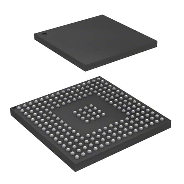
- Package: 119-ball BGA package
- Essence: Memory chip for storing and retrieving data
- Packaging/Quantity: Available in reels of 250 units
Specifications
- Memory Size: 4 Megabits (512K x 8)
- Operating Voltage: 3.3V
- Access Time: 5 ns
- Operating Temperature Range: -40°C to +85°C
- Data Retention: 10 years
- Interface: Synchronous
Detailed Pin Configuration
The IDT72T40118L5BB has a total of 119 pins. The pin configuration is as follows:
- VDDQ
- VSSQ
- NC
- A0
- A1
- A2
- A3
- A4
- A5
- A6
- A7
- A8
- A9
- A10
- A11
- A12
- A13
- A14
- A15
- A16
- A17
- A18
- A19
- A20
- A21
- A22
- A23
- A24
- A25
- A26
- A27
- A28
- A29
- A30
- A31
- A32
- A33
- A34
- A35
- A36
- A37
- A38
- A39
- A40
- A41
- A42
- A43
- A44
- A45
- A46
- A47
- A48
- A49
- A50
- A51
- A52
- A53
- A54
- A55
- A56
- A57
- A58
- A59
- A60
- A61
- A62
- A63
- A64
- A65
- A66
- A67
- A68
- A69
- A70
- A71
- A72
- A73
- A74
- A75
- A76
- A77
- A78
- A79
- A80
- A81
- A82
- A83
- A84
- A85
- A86
- A87
- A88
- A89
- A90
- A91
- A92
- A93
- A94
- A95
- A96
- A97
- A98
- A99
- A100
- A101
- A102
- A103
- A104
- A105
- A106
- A107
- A108
- A109
- A110
- A111
- A112
- A113
- A114
- VDD
Functional Features
- High-speed synchronous operation
- Low-power consumption
- Byte-write and page-write capability
- Automatic power-down mode
- Output enable and write enable control signals
- Internal burst counter for sequential access
Advantages and Disadvantages
Advantages: - High-speed operation allows for quick data retrieval - Low-power consumption helps conserve energy - Byte-write and page-write capability enhance flexibility - Automatic power-down mode saves power when not in use - Output enable and write enable control signals provide efficient data management - Internal burst counter enables sequential access, improving efficiency
Disadvantages: - Limited memory size (4 Megabits) - Synchronous interface may require additional synchronization circuitry in certain applications
Working Principles
The IDT72T40118L5BB is a synchronous static random-access memory (SRAM) chip. It stores and retrieves data using an internal array of memory cells. The synchronous operation ensures that data is read or written at specific clock cycles, allowing for high-speed operation. The chip
技術ソリューションにおける IDT72T40118L5BB の適用に関連する 10 件の一般的な質問と回答をリストします。
Sure! Here are 10 common questions and answers related to the application of IDT72T40118L5BB in technical solutions:
Q: What is IDT72T40118L5BB? A: IDT72T40118L5BB is a high-speed, low-power, 18-bit synchronous dual-port RAM designed for use in various technical applications.
Q: What are the key features of IDT72T40118L5BB? A: Some key features include a maximum clock frequency of 166 MHz, 18-bit data width, dual-port architecture, and low power consumption.
Q: How can IDT72T40118L5BB be used in technical solutions? A: It can be used as a memory buffer, data storage, or for interprocessor communication in systems that require high-speed and reliable data transfer.
Q: What is the maximum clock frequency supported by IDT72T40118L5BB? A: The maximum clock frequency supported is 166 MHz, allowing for fast data transfers and efficient operation.
Q: Can IDT72T40118L5BB be used in multi-processor systems? A: Yes, it is designed for use in multi-processor systems where multiple processors need to access shared memory simultaneously.
Q: Does IDT72T40118L5BB support simultaneous read and write operations? A: Yes, it supports simultaneous read and write operations on both ports, enabling efficient data transfer between different components.
Q: What is the power consumption of IDT72T40118L5BB? A: The power consumption is relatively low, making it suitable for battery-powered devices or applications with strict power constraints.
Q: Can IDT72T40118L5BB be cascaded to increase memory capacity? A: Yes, multiple IDT72T40118L5BB devices can be cascaded together to increase the overall memory capacity in a system.
Q: Does IDT72T40118L5BB have any built-in error detection or correction mechanisms? A: No, it does not have built-in error detection or correction mechanisms. Additional error checking mechanisms may need to be implemented if required.
Q: What are some typical applications of IDT72T40118L5BB? A: Some typical applications include networking equipment, telecommunications systems, high-performance computing, and industrial automation.
Please note that these answers are general and may vary depending on specific requirements and use cases.