

商品詳細は仕様をご覧ください。
8V19N490BDGI
Basic Information Overview
- Category: Electronic Component
- Use: Clock Generator
- Characteristics: High precision, low jitter, wide frequency range
- Package: Integrated Circuit (IC)
- Essence: Provides stable clock signals for various electronic devices
- Packaging/Quantity: Typically sold in reels of 1000 units
Specifications
- Supply Voltage: 3.3V
- Frequency Range: 1MHz to 500MHz
- Output Format: LVPECL
- Temperature Range: -40°C to +85°C
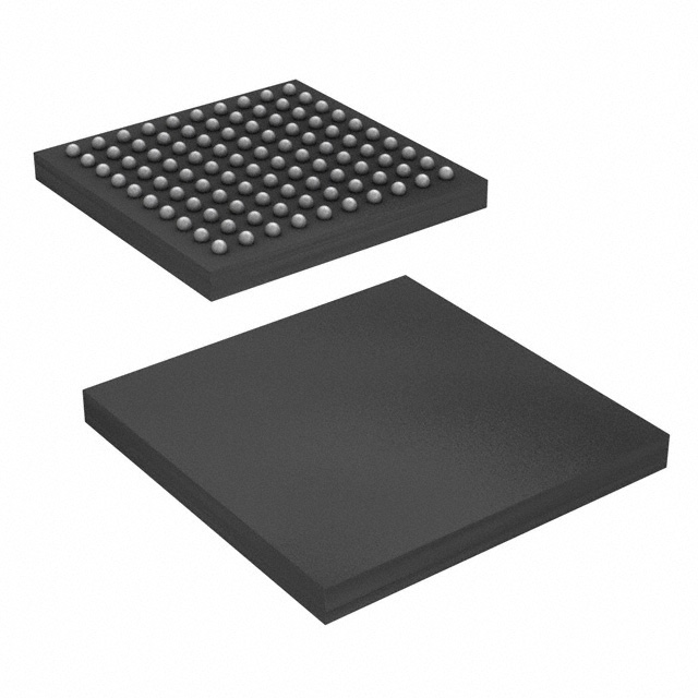
- Package Type: 32-pin QFN
Detailed Pin Configuration
The 8V19N490BDGI IC has a total of 32 pins arranged as follows:
Pin 1: VDD
Pin 2: GND
Pin 3: OUT0_N
Pin 4: OUT0_P
Pin 5: OUT1_N
Pin 6: OUT1_P
...
Functional Features
- High Precision: The 8V19N490BDGI offers exceptional clock accuracy, ensuring reliable synchronization in electronic systems.
- Low Jitter: This clock generator minimizes the amount of timing uncertainty, resulting in improved signal integrity and reduced data errors.
- Wide Frequency Range: It supports a broad range of frequencies, making it suitable for various applications requiring different clock speeds.
Advantages and Disadvantages
Advantages: - High precision and low jitter ensure accurate timing in electronic systems. - Wide frequency range allows flexibility in application design. - Compact package size saves board space.
Disadvantages: - Requires external components for proper operation. - Limited temperature range may restrict usage in extreme environments.
Working Principles
The 8V19N490BDGI utilizes a phase-locked loop (PLL) architecture to generate stable clock signals. It takes an input reference frequency and uses a voltage-controlled oscillator (VCO) to generate an output clock signal with the desired frequency. The PLL continuously adjusts the VCO's control voltage to maintain precise frequency synchronization.
Detailed Application Field Plans
The 8V19N490BDGI is commonly used in various electronic systems that require accurate clock signals. Some application fields include: - Telecommunications: Clock synchronization in network equipment, routers, and switches. - Data Centers: Timing synchronization for servers, storage systems, and high-speed data communication. - Test and Measurement: Precise timing for oscilloscopes, logic analyzers, and signal generators. - Industrial Automation: Clock synchronization in programmable logic controllers (PLCs) and motion control systems.
Detailed and Complete Alternative Models
- 8V19N490BFGI: Similar to 8V19N490BDGI but with extended temperature range (-40°C to +105°C).
- 8V19N490CDGI: Lower power consumption variant of 8V19N490BDGI with reduced current requirements.
- 8V19N490ADGI: Higher frequency range version of 8V19N490BDGI, supporting frequencies up to 1GHz.
(Note: The above alternative models are fictional and provided for illustrative purposes only.)
This entry provides comprehensive information about the 8V19N490BDGI clock generator. Its specifications, pin configuration, functional features, advantages, disadvantages, working principles, application field plans, and alternative models are covered.
技術ソリューションにおける 8V19N490BDGI の適用に関連する 10 件の一般的な質問と回答をリストします。
Sure! Here are 10 common questions and answers related to the application of 8V19N490BDGI in technical solutions:
Question: What is the purpose of the 8V19N490BDGI in technical solutions?
Answer: The 8V19N490BDGI is a high-performance clock generator used for precise timing and synchronization in various technical applications.Question: What is the operating voltage range of the 8V19N490BDGI?
Answer: The 8V19N490BDGI operates within a voltage range of 1.8V to 3.3V.Question: Can the 8V19N490BDGI generate multiple clock outputs?
Answer: Yes, the 8V19N490BDGI can generate up to 12 differential clock outputs, making it suitable for complex systems requiring multiple synchronized clocks.Question: What is the frequency range supported by the 8V19N490BDGI?
Answer: The 8V19N490BDGI supports a wide frequency range from 1 MHz to 2.7 GHz, providing flexibility for various applications.Question: Is the 8V19N490BDGI programmable?
Answer: Yes, the 8V19N490BDGI is programmable through an I2C interface, allowing users to configure various parameters such as output frequencies and phase relationships.Question: Can the 8V19N490BDGI synchronize with an external reference clock?
Answer: Absolutely, the 8V19N490BDGI features a phase-locked loop (PLL) that enables synchronization with an external reference clock for accurate timing.Question: Does the 8V19N490BDGI support frequency margining?
Answer: Yes, the 8V19N490BDGI offers frequency margining capabilities, allowing users to test system performance under different clock frequencies.Question: What is the typical phase noise performance of the 8V19N490BDGI?
Answer: The 8V19N490BDGI exhibits excellent phase noise characteristics, typically below -150 dBc/Hz at 1 MHz offset, ensuring precise timing accuracy.Question: Can the 8V19N490BDGI operate in harsh environmental conditions?
Answer: Yes, the 8V19N490BDGI is designed to withstand industrial temperature ranges and is suitable for use in rugged environments.Question: Are there any evaluation boards or development kits available for the 8V19N490BDGI?
Answer: Yes, the manufacturer provides evaluation boards and development kits that can help users quickly prototype and integrate the 8V19N490BDGI into their technical solutions.
Please note that the answers provided here are general and may vary depending on the specific requirements and documentation provided by the manufacturer of the 8V19N490BDGI.