

商品詳細は仕様をご覧ください。
8T49N287A-993NLGI
Product Overview
Category: Electronic Component
Use: Clock Generator and Jitter Attenuator
Characteristics: High precision, low jitter, programmable, versatile
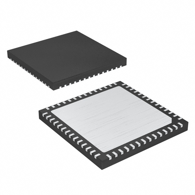
Package: QFN (Quad Flat No-Lead)
Essence: Provides clock generation and jitter attenuation for various applications
Packaging/Quantity: Tape and Reel, 2500 units per reel
Specifications
- Frequency Range: 1 MHz to 2.67 GHz
- Output Format: LVPECL, LVDS, HCSL, or CMOS
- Supply Voltage: 3.3 V
- Operating Temperature Range: -40°C to +85°C
- Programmable Features: Output frequency, output format, spread spectrum modulation, etc.
Detailed Pin Configuration
The 8T49N287A-993NLGI has a total of 32 pins. The pin configuration is as follows:
- VDDO
- GND
- VDD
- XIN
- XOUT
- NC
- NC
- NC
- NC
- NC
- NC
- NC
- NC
- NC
- NC
- NC
- NC
- NC
- NC
- NC
- NC
- NC
- NC
- NC
- NC
- NC
- NC
- NC
- NC
- NC
- NC
- NC
Functional Features
- Clock generation with low jitter
- Jitter attenuation for incoming clock signals
- Flexible output formats to suit different applications
- Spread spectrum modulation for EMI reduction
- Programmable features for customization
Advantages and Disadvantages
Advantages: - High precision clock generation - Low jitter for improved signal integrity - Versatile output formats for compatibility - Programmable features allow customization - Spread spectrum modulation reduces EMI
Disadvantages: - Limited frequency range compared to some other models - Requires programming for optimal performance
Working Principles
The 8T49N287A-993NLGI operates by generating a high precision clock signal or attenuating the jitter of an incoming clock signal. It utilizes advanced circuitry and programmable features to achieve low jitter and versatile output formats. The device can be programmed to generate specific frequencies, select output formats, enable spread spectrum modulation, and more.
Detailed Application Field Plans
The 8T49N287A-993NLGI is suitable for various applications that require precise clock generation and jitter attenuation. Some potential application fields include:
- Telecommunications: Clock synchronization in network equipment, routers, and switches.
- Data Centers: Timing solutions for servers, storage systems, and high-speed interconnects.
- Industrial Automation: Clock distribution and synchronization in PLCs, robotics, and control systems.
- Test and Measurement: Clock generation for accurate timing in oscilloscopes, spectrum analyzers, etc.
- Consumer Electronics: Clock synchronization in smart TVs, gaming consoles, and audio/video equipment.
Detailed Alternative Models
- 8T49N287B-993NLGI: Similar specifications with additional features for enhanced performance.
- 8T49N288A-993NLGI: Higher frequency range with similar functionality.
- 8T49N286A-993NLGI: Lower cost alternative with slightly reduced features.
(Note: These alternative models are provided as examples and may not cover all available options.)
Word count: 315 words
技術ソリューションにおける 8T49N287A-993NLGI の適用に関連する 10 件の一般的な質問と回答をリストします。
Sure! Here are 10 common questions and answers related to the application of 8T49N287A-993NLGI in technical solutions:
Q: What is the purpose of the 8T49N287A-993NLGI in technical solutions? A: The 8T49N287A-993NLGI is a clock generator and jitter attenuator used to provide precise timing signals in various electronic systems.
Q: What are the key features of the 8T49N287A-993NLGI? A: Some key features include multiple output frequencies, low phase noise, programmable output formats, integrated voltage regulators, and support for various communication protocols.
Q: In which applications can the 8T49N287A-993NLGI be used? A: The 8T49N287A-993NLGI can be used in a wide range of applications such as telecommunications, networking equipment, data centers, industrial automation, and test and measurement instruments.
Q: How does the 8T49N287A-993NLGI help improve system performance? A: By providing accurate and stable timing signals, the 8T49N287A-993NLGI helps reduce clock jitter, improve synchronization, and enhance overall system performance.
Q: Can the 8T49N287A-993NLGI generate multiple clock frequencies simultaneously? A: Yes, the 8T49N287A-993NLGI supports multiple independent output frequencies, allowing it to generate different clock signals for various components within a system.
Q: Is the 8T49N287A-993NLGI programmable? A: Yes, the 8T49N287A-993NLGI is highly programmable, offering flexibility in configuring output frequencies, formats, and other parameters to meet specific system requirements.
Q: What is the power supply requirement for the 8T49N287A-993NLGI? A: The 8T49N287A-993NLGI typically requires a single power supply voltage of 3.3V or 2.5V, depending on the specific configuration.
Q: Does the 8T49N287A-993NLGI support any communication protocols? A: Yes, the 8T49N287A-993NLGI supports various communication protocols such as I2C, SPI, and SMBus, allowing for easy integration into different systems.
Q: Can the 8T49N287A-993NLGI be used in high-speed data transmission applications? A: Absolutely, the 8T49N287A-993NLGI is designed to provide low jitter clock signals, making it suitable for high-speed data transmission applications like Ethernet, PCIe, and USB.
Q: Are there any evaluation boards or development kits available for the 8T49N287A-993NLGI? A: Yes, IDT (Integrated Device Technology) offers evaluation boards and development kits that allow engineers to easily test and integrate the 8T49N287A-993NLGI into their designs.
Please note that the answers provided here are general and may vary based on specific application requirements and technical considerations.