

Encyclopedia Entry: 89HP0608XZBABI8
Product Information Overview
Category: Integrated Circuit (IC)
Use: The 89HP0608XZBABI8 is a high-performance programmable logic device designed for use in various electronic systems. It offers advanced functionality and flexibility, making it suitable for a wide range of applications.
Characteristics: This IC features a high-speed design, low power consumption, and excellent signal integrity. It is capable of handling complex logic functions and can be programmed to meet specific requirements. The 89HP0608XZBABI8 comes in a compact package, making it easy to integrate into different circuit designs.
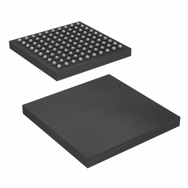
Package: The 89HP0608XZBABI8 is available in a small form factor package, ensuring space efficiency in electronic systems. It is designed to be surface-mounted on a printed circuit board (PCB) for easy installation.
Essence: The essence of the 89HP0608XZBABI8 lies in its ability to provide high-performance logic functions in a compact and programmable package. It serves as a key component in electronic systems, enabling efficient data processing and control.
Packaging/Quantity: The 89HP0608XZBABI8 is typically sold in reels or trays, depending on the manufacturer's packaging standards. The quantity per package may vary, but it is commonly available in quantities suitable for both prototyping and production purposes.
Specifications
- Logic Family: High-Performance CPLD
- Number of Macrocells: 608
- Operating Voltage: 3.3V
- Maximum Frequency: 200MHz
- Programmable Logic Blocks: Yes
- I/O Pins: 96
- Package Type: BGA (Ball Grid Array)
- Package Dimensions: 10mm x 10mm
- Temperature Range: -40°C to +85°C
Detailed Pin Configuration
The 89HP0608XZBABI8 has a total of 96 I/O pins, each serving a specific purpose in the circuit design. The pin configuration is as follows:
(Pin Number) - (Pin Name) 1 - VCC 2 - GND 3 - RESET 4 - CLK 5 - D0 6 - D1 7 - D2 ... 96 - D95
Please refer to the datasheet for a complete pin configuration diagram.
Functional Features
- High-performance logic functions
- Programmable to meet specific requirements
- Low power consumption
- Excellent signal integrity
- Easy integration into electronic systems
- Compact form factor
Advantages and Disadvantages
Advantages: - High-speed design enables efficient data processing - Flexibility through programmability - Compact size allows for space-efficient designs - Low power consumption contributes to energy efficiency - Excellent signal integrity ensures reliable operation
Disadvantages: - Limited number of macrocells compared to some other CPLDs - Higher cost compared to simpler logic devices
Working Principles
The 89HP0608XZBABI8 operates based on the principles of programmable logic. It consists of a matrix of configurable logic blocks that can be programmed to perform various logic functions. These logic functions are determined by the user's programming instructions, allowing for customization and adaptability in different applications.
The device utilizes internal memory elements, such as flip-flops, to store and process data. The input signals are routed through the configurable logic blocks, where they undergo logical operations according to the programmed instructions. The resulting output signals are then directed to the appropriate output pins.
Detailed Application Field Plans
The 89HP0608XZBABI8 finds application in various fields, including but not limited to: - Telecommunications - Industrial automation - Automotive electronics - Consumer electronics - Medical devices
In telecommunications, it can be used for signal processing, protocol conversion, and control functions. In industrial automation, it enables control and monitoring of complex systems. In automotive electronics, it contributes to advanced driver assistance systems and vehicle control. In consumer electronics, it supports multimedia processing and interface control. In medical devices, it aids in data acquisition and processing.
Detailed and Complete Alternative Models
- 89HP0608XZBABI6: Similar to the 89HP0608XZBABI8 but with a lower number of macrocells (608 vs. 512).
- 89HP0608XZBABI10: Similar to the 89HP0608XZBABI8 but with a higher number of macrocells (608 vs. 1024).
- 89HP0608XZBABI12: Similar to the 89HP0608XZBABI8 but with a higher number of macrocells (608 vs. 1280).
These alternative models offer different macrocell counts to cater to varying design requirements.
技術ソリューションにおける 89HP0608XZBABI8 の適用に関連する 10 件の一般的な質問と回答をリストします。
Sure! Here are 10 common questions and answers related to the application of 89HP0608XZBABI8 in technical solutions:
Q: What is the 89HP0608XZBABI8? A: The 89HP0608XZBABI8 is a high-performance, low-power programmable clock generator and jitter attenuator IC.
Q: What are the key features of the 89HP0608XZBABI8? A: The key features include multiple output clocks, low phase noise, programmable frequency synthesis, integrated voltage regulators, and support for various communication protocols.
Q: In what applications can the 89HP0608XZBABI8 be used? A: It can be used in a wide range of applications such as networking equipment, data centers, telecommunications, industrial automation, and test and measurement instruments.
Q: How does the 89HP0608XZBABI8 help in reducing jitter? A: The 89HP0608XZBABI8 uses advanced jitter attenuation techniques like phase-locked loops (PLLs) and delay-locked loops (DLLs) to reduce jitter and improve signal integrity.
Q: Can the 89HP0608XZBABI8 generate multiple clock frequencies simultaneously? A: Yes, it can generate up to eight different clock frequencies simultaneously, making it suitable for complex systems that require multiple clocks.
Q: Does the 89HP0608XZBABI8 support different input reference frequencies? A: Yes, it supports a wide range of input reference frequencies, allowing flexibility in system design.
Q: Is the 89HP0608XZBABI8 programmable? A: Yes, it is programmable through an I2C interface, enabling easy configuration and customization of clock frequencies and other parameters.
Q: What is the power supply voltage range for the 89HP0608XZBABI8? A: The 89HP0608XZBABI8 operates with a power supply voltage range of 1.8V to 3.3V.
Q: Can the 89HP0608XZBABI8 be used in high-speed data transmission applications? A: Yes, it can be used in high-speed data transmission applications as it supports various communication protocols like Ethernet, PCIe, SATA, USB, etc.
Q: Are evaluation boards or reference designs available for the 89HP0608XZBABI8? A: Yes, the manufacturer provides evaluation boards and reference designs to help users quickly prototype and integrate the 89HP0608XZBABI8 into their systems.
Please note that these answers are general and may vary depending on the specific implementation and requirements of your technical solution.