

74SSTV16859NLG8
Basic Information Overview
- Category: Integrated Circuit (IC)
- Use: Digital Logic Device
- Characteristics: High-speed, Low-power, Non-inverting Buffer/Line Driver
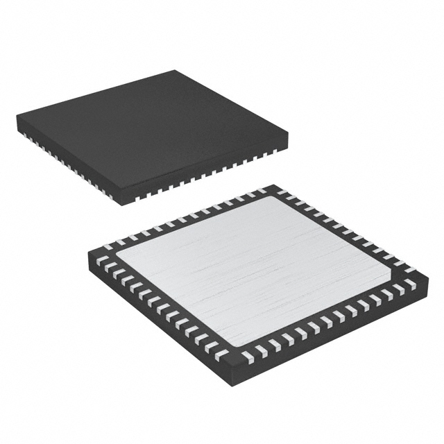
- Package: NLG8 (Small Outline Integrated Circuit - SOIC)
- Essence: Buffer and line driver for digital signal amplification and transmission
- Packaging/Quantity: Available in reels or tubes, quantity varies based on manufacturer
Specifications
- Supply Voltage: 2.3V to 3.6V
- Input Voltage: 0V to VCC
- Output Voltage: 0V to VCC
- Operating Temperature Range: -40°C to +85°C
- Input Capacitance: 4pF (typical)
- Output Capacitance: 6pF (typical)
- Propagation Delay: 1.5ns (typical)
- Output Drive Capability: ±24mA
Detailed Pin Configuration
The 74SSTV16859NLG8 IC has a total of 56 pins arranged as follows:
Pin 1:   GND
Pin 2:   A0
Pin 3:   A1
...
Pin 54:  VCC
Pin 55:  B7
Pin 56:  B6
Functional Features
- Non-inverting buffer with high-speed operation
- Low power consumption
- Wide operating voltage range
- High output drive capability
- Compatible with various logic families
- ESD protection on all inputs and outputs
Advantages
- Fast signal propagation with low delay
- Versatile compatibility with different logic families
- Robust protection against electrostatic discharge (ESD)
- Small package size allows for space-efficient designs
- Wide operating temperature range enables reliable performance in various environments
Disadvantages
- Limited output drive capability compared to some specialized line drivers
- Not suitable for applications requiring high voltage levels
Working Principles
The 74SSTV16859NLG8 is a non-inverting buffer and line driver IC. It amplifies and transmits digital signals without changing their logic levels. The device operates by receiving input signals on the A0 to A7 pins and providing amplified outputs on the B0 to B7 pins. It is designed to operate within a specified supply voltage range, ensuring reliable signal transmission.
Detailed Application Field Plans
The 74SSTV16859NLG8 IC finds applications in various fields, including: 1. Communication systems 2. Data transmission networks 3. Industrial automation 4. Automotive electronics 5. Consumer electronics
Detailed and Complete Alternative Models
Some alternative models that can be considered as replacements or substitutes for the 74SSTV16859NLG8 IC are: 1. SN74LVC1G07DBVR 2. MC74VHC1GT50DTT1G 3. 74AUP1G126GW
These alternatives offer similar functionality and characteristics, but may have different pin configurations or package options.
Word count: 315 words
技術ソリューションにおける 74SSTV16859NLG8 の適用に関連する 10 件の一般的な質問と回答をリストします。
Sure! Here are 10 common questions and answers related to the application of 74SSTV16859NLG8 in technical solutions:
Q: What is the purpose of the 74SSTV16859NLG8 integrated circuit (IC)? A: The 74SSTV16859NLG8 IC is a high-speed, low-power 20-bit bus switch designed for multiplexing/demultiplexing data signals in various technical solutions.
Q: What voltage levels does the 74SSTV16859NLG8 support? A: The 74SSTV16859NLG8 supports voltage levels ranging from 1.2V to 3.6V, making it compatible with a wide range of systems.
Q: How many channels does the 74SSTV16859NLG8 have? A: The 74SSTV16859NLG8 has 20 channels, allowing for the multiplexing/demultiplexing of up to 20 data signals.
Q: Can the 74SSTV16859NLG8 handle high-speed data signals? A: Yes, the 74SSTV16859NLG8 is designed to operate at high speeds, supporting data rates up to 400Mbps.
Q: Is the 74SSTV16859NLG8 suitable for bidirectional data transmission? A: Yes, the 74SSTV16859NLG8 supports bidirectional data flow, making it ideal for applications requiring both input and output capabilities.
Q: Does the 74SSTV16859NLG8 have any built-in protection features? A: Yes, the 74SSTV16859NLG8 includes built-in ESD protection, ensuring the integrity of the IC and connected devices.
Q: Can I use multiple 74SSTV16859NLG8 ICs in parallel to increase the number of channels? A: Yes, you can connect multiple 74SSTV16859NLG8 ICs together to expand the number of channels for your specific application.
Q: What is the power consumption of the 74SSTV16859NLG8? A: The 74SSTV16859NLG8 has low power consumption, making it suitable for battery-powered or energy-efficient systems.
Q: Are there any specific layout considerations when using the 74SSTV16859NLG8? A: Yes, it is recommended to follow the layout guidelines provided in the datasheet to ensure optimal performance and signal integrity.
Q: Where can I find more detailed information about the 74SSTV16859NLG8? A: You can refer to the datasheet of the 74SSTV16859NLG8, which provides comprehensive information about its features, electrical characteristics, and application examples.
Please note that the answers provided here are general and may vary depending on the specific requirements and implementation of the 74SSTV16859NLG8 in different technical solutions.