

Encyclopedia Entry: 74FCT162501CTPVG8
Product Information Overview
- Category: Integrated Circuit (IC)
- Use: Logic Level Shifter
- Characteristics: High-speed, bidirectional voltage level translation
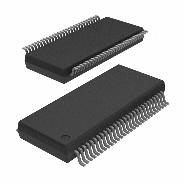
- Package: TSSOP-48
- Essence: Translates signals between different voltage levels
- Packaging/Quantity: Available in reels of 2500 units
Specifications
- Logic Family: FCT
- Number of Bits: 16
- Input Voltage Range: 2.0V to 5.5V
- Output Voltage Range: 2.0V to 5.5V
- Propagation Delay: 3.5ns (typical)
- Operating Temperature Range: -40°C to +85°C
Detailed Pin Configuration
The 74FCT162501CTPVG8 IC has a total of 48 pins arranged as follows:
- OE (Output Enable) Pin 1
- A1 (Input A1) Pin 2
- B1 (Input B1) Pin 3
- Y1 (Output Y1) Pin 4
- GND (Ground) Pin 5
- Y2 (Output Y2) Pin 6
- B2 (Input B2) Pin 7
- A2 (Input A2) Pin 8
- VCC (Power Supply) Pin 9
- OE (Output Enable) Pin 10
- A3 (Input A3) Pin 11
- B3 (Input B3) Pin 12
- Y3 (Output Y3) Pin 13
- GND (Ground) Pin 14
- Y4 (Output Y4) Pin 15
- B4 (Input B4) Pin 16
- A4 (Input A4) Pin 17
- VCC (Power Supply) Pin 18
- OE (Output Enable) Pin 19
- A5 (Input A5) Pin 20
- B5 (Input B5) Pin 21
- Y5 (Output Y5) Pin 22
- GND (Ground) Pin 23
- Y6 (Output Y6) Pin 24
- B6 (Input B6) Pin 25
- A6 (Input A6) Pin 26
- VCC (Power Supply) Pin 27
- OE (Output Enable) Pin 28
- A7 (Input A7) Pin 29
- B7 (Input B7) Pin 30
- Y7 (Output Y7) Pin 31
- GND (Ground) Pin 32
- Y8 (Output Y8) Pin 33
- B8 (Input B8) Pin 34
- A8 (Input A8) Pin 35
- VCC (Power Supply) Pin 36
- OE (Output Enable) Pin 37
- A9 (Input A9) Pin 38
- B9 (Input B9) Pin 39
- Y9 (Output Y9) Pin 40
- GND (Ground) Pin 41
- Y10 (Output Y10) Pin 42
- B10 (Input B10) Pin 43
- A10 (Input A10) Pin 44
- VCC (Power Supply) Pin 45
- OE (Output Enable) Pin 46
- A11 (Input A11) Pin 47
- B11 (Input B11) Pin 48
Functional Features
- Bidirectional voltage level translation between two different voltage domains
- High-speed operation with low propagation delay
- Output enable control for easy signal routing and isolation
Advantages and Disadvantages
Advantages: - Enables seamless communication between devices operating at different voltage levels - Fast signal transmission with minimal delay - Compact package size for space-constrained applications
Disadvantages: - Requires careful consideration of input and output voltage compatibility - Limited to a specific number of bits (16 in this case)
Working Principles
The 74FCT162501CTPVG8 is a logic level shifter that facilitates the translation of signals between two different voltage domains. It operates bidirectionally, allowing signals to be transmitted from one domain to another and vice versa. The IC utilizes internal circuitry to ensure proper voltage level shifting while maintaining signal integrity.
Detailed Application Field Plans
The 74FCT162501CTPVG8 finds application in
技術ソリューションにおける 74FCT162501CTPVG8 の適用に関連する 10 件の一般的な質問と回答をリストします。
Sure! Here are 10 common questions and answers related to the application of 74FCT162501CTPVG8 in technical solutions:
Q: What is the 74FCT162501CTPVG8? A: The 74FCT162501CTPVG8 is a 16-bit registered transceiver with 3-state outputs, designed for high-performance bus interface applications.
Q: What is the operating voltage range of the 74FCT162501CTPVG8? A: The operating voltage range of the 74FCT162501CTPVG8 is typically between 4.5V and 5.5V.
Q: What is the maximum data transfer rate supported by the 74FCT162501CTPVG8? A: The 74FCT162501CTPVG8 supports a maximum data transfer rate of up to 200 MHz.
Q: Can the 74FCT162501CTPVG8 be used as a bidirectional buffer? A: Yes, the 74FCT162501CTPVG8 can be used as a bidirectional buffer, allowing data to flow in both directions.
Q: How many output enable pins does the 74FCT162501CTPVG8 have? A: The 74FCT162501CTPVG8 has two output enable pins, OEAB and OEBA, which control the direction of data flow.
Q: What is the typical propagation delay of the 74FCT162501CTPVG8? A: The typical propagation delay of the 74FCT162501CTPVG8 is around 3.5 ns.
Q: Can the 74FCT162501CTPVG8 be used in a hot-swappable application? A: Yes, the 74FCT162501CTPVG8 is designed to support hot-swapping, allowing for easy replacement or insertion of modules without disrupting the system.
Q: What is the maximum output current that the 74FCT162501CTPVG8 can drive? A: The 74FCT162501CTPVG8 can drive up to 48 mA of output current per pin.
Q: Does the 74FCT162501CTPVG8 have any built-in ESD protection? A: Yes, the 74FCT162501CTPVG8 has built-in ESD protection, which helps safeguard against electrostatic discharge events.
Q: Can the 74FCT162501CTPVG8 be cascaded with other similar devices? A: Yes, the 74FCT162501CTPVG8 can be cascaded with other similar devices to expand the number of input/output lines in a system.
Please note that these answers are general and may vary depending on specific datasheet specifications and application requirements.