

Encyclopedia Entry: 74FCT16244CTPVG
Product Overview
Category
The 74FCT16244CTPVG belongs to the category of integrated circuits (ICs).
Use
This IC is commonly used in electronic devices for signal amplification and buffering purposes.
Characteristics
- The 74FCT16244CTPVG is a high-speed, low-power octal buffer/line driver.
- It operates at a voltage range of 4.5V to 5.5V.
- This IC offers non-inverting outputs and tri-state outputs for bus-oriented applications.
- It provides balanced propagation delays and transition times, making it suitable for high-performance systems.
Package
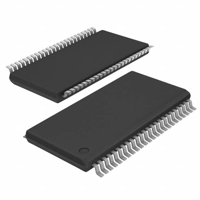
The 74FCT16244CTPVG is available in a 48-pin TSSOP (Thin Shrink Small Outline Package) package.
Essence
The essence of the 74FCT16244CTPVG lies in its ability to amplify and buffer signals effectively, ensuring reliable data transmission within electronic systems.
Packaging/Quantity
This IC is typically sold in reels or tubes, with each reel containing approximately 2500 units.
Specifications
- Supply Voltage Range: 4.5V to 5.5V
- Input Voltage Range: 0V to VCC
- Output Voltage Range: 0V to VCC
- Operating Temperature Range: -40°C to +85°C
- Maximum Propagation Delay: 6ns
- Maximum Output Current: ±24mA
Detailed Pin Configuration
The 74FCT16244CTPVG has a total of 48 pins, which are assigned specific functions. Here is a detailed pin configuration:
- OE (Output Enable) 1
- Y1 (Output) 1
- A1 (Input) 1
- GND (Ground)
- A2 (Input) 2
- Y2 (Output) 2
- OE (Output Enable) 2
- VCC (Supply Voltage)
- Y3 (Output) 3
- A3 (Input) 3
- GND (Ground)
- A4 (Input) 4
- Y4 (Output) 4
- OE (Output Enable) 3
- VCC (Supply Voltage)
- Y5 (Output) 5
- A5 (Input) 5
- GND (Ground)
- A6 (Input) 6
- Y6 (Output) 6
- OE (Output Enable) 4
- VCC (Supply Voltage)
- Y7 (Output) 7
- A7 (Input) 7
- GND (Ground)
- A8 (Input) 8
- Y8 (Output) 8
- OE (Output Enable) 5
- VCC (Supply Voltage)
- Y9 (Output) 9
- A9 (Input) 9
- GND (Ground)
- A10 (Input) 10
- Y10 (Output) 10
- OE (Output Enable) 6
- VCC (Supply Voltage)
- Y11 (Output) 11
- A11 (Input) 11
- GND (Ground)
- A12 (Input) 12
- Y12 (Output) 12
- OE (Output Enable) 7
- VCC (Supply Voltage)
- Y13 (Output) 13
- A13 (Input) 13
- GND (Ground)
- A14 (Input) 14
- Y14 (Output) 14
Functional Features
- The 74FCT16244CTPVG provides eight non-inverting buffer/line driver channels.
- It offers tri-state outputs, allowing multiple devices to share a common bus.
- This IC has balanced propagation delays and transition times, ensuring reliable data transmission in high-speed systems.
- It operates at a low power supply voltage, making it suitable for battery-powered applications.
Advantages and Disadvantages
Advantages
- High-speed operation enables efficient data transfer.
- Tri-state outputs facilitate bus sharing among multiple devices.
- Low power consumption enhances energy efficiency.
- Balanced propagation delays ensure accurate signal synchronization.
Disadvantages
- Limited output current may restrict its use in certain high-current applications.
- The 48-pin TSSOP package may require specialized equipment for soldering and handling.
Working Principles
The 74FCT16244CTPVG functions as a buffer/line driver by amplifying and buffering input signals. When the output enable (OE)
技術ソリューションにおける 74FCT16244CTPVG の適用に関連する 10 件の一般的な質問と回答をリストします。
Sure! Here are 10 common questions and answers related to the application of 74FCT16244CTPVG in technical solutions:
Q: What is the 74FCT16244CTPVG? A: The 74FCT16244CTPVG is a 16-bit buffer/line driver with 3-state outputs, commonly used in digital logic circuits.
Q: What is the voltage supply range for the 74FCT16244CTPVG? A: The voltage supply range for this IC is typically between 4.5V and 5.5V.
Q: What is the maximum operating frequency of the 74FCT16244CTPVG? A: The maximum operating frequency of this IC is typically around 200 MHz.
Q: Can the 74FCT16244CTPVG be used as a level shifter? A: Yes, it can be used as a level shifter to convert signals between different voltage levels.
Q: How many output pins does the 74FCT16244CTPVG have? A: This IC has 16 output pins, each capable of driving a single line.
Q: Is the 74FCT16244CTPVG compatible with TTL logic levels? A: Yes, it is compatible with both TTL and CMOS logic levels.
Q: What is the typical output current capability of the 74FCT16244CTPVG? A: The typical output current capability is around 24 mA per output pin.
Q: Can the 74FCT16244CTPVG be used in bidirectional data transfer applications? A: Yes, it can be used for bidirectional data transfer by enabling the 3-state outputs.
Q: Does the 74FCT16244CTPVG have built-in protection against electrostatic discharge (ESD)? A: Yes, it typically has ESD protection to prevent damage from static electricity.
Q: What is the package type for the 74FCT16244CTPVG? A: The 74FCT16244CTPVG is commonly available in a 48-pin TSSOP (Thin Shrink Small Outline Package) format.
Please note that the answers provided here are general and may vary depending on the specific datasheet and manufacturer's specifications for the 74FCT16244CTPVG.